Semiconductor device and IC card

a technology of semiconductor devices and ic cards, applied in the field of semiconductor devices, can solve problems such as malfunction due to characteristic degradation, device breakage, and change of signal processing circuit characteristics

Inactive Publication Date: 2007-01-30
RENESAS ELECTRONICS CORP
View PDF5 Cites 4 Cited by
  • Summary
  • Abstract
  • Description
  • Claims
  • Application Information

AI Technical Summary

Benefits of technology

[0011]The typical ones of the inventions disclosed in this application will be briefly described as follows. That is, an IC card in which an internal circuit is operated by an internal power supply formed in a voltage controlling circuit by alternate current from outside received by an antenna is provided, in which the operation of the internal circuit is controlled by the operating current detector circuit which detects the supplied current of the internal power supply. Here, the voltage controlling circuit of the present invention includes a voltage controlling current source, and when the current higher than a predetermined current I1 flows in the voltage controlling current source while the internal circuit is not operated, the operating current detector circuit outputs an enabling signal. When the internal circuit is operated by receiving the enabling signal, the current I1 consumed in the internal circuit is subtracted from the current passing through the voltage controlling current source. As a result, since the change in current in the whole internal power supply can be prevented, the output voltage of the internal power supply can be kept constant practically.

Problems solved by technology

In this case, when excessive power is supplied from the interrogator and the power supply voltage higher than the withstand voltage of the devices constituting the internal circuit is supplied, the devices are broken.
Consequently, there is the possibility that the characteristics of the signal processing circuit are changed and the malfunction due to the characteristic degradation occurs.

Method used


Image

  • Semiconductor device and IC card
  • Semiconductor device and IC card
  • Semiconductor device and IC card

Examples


first embodiment

(First Embodiment)

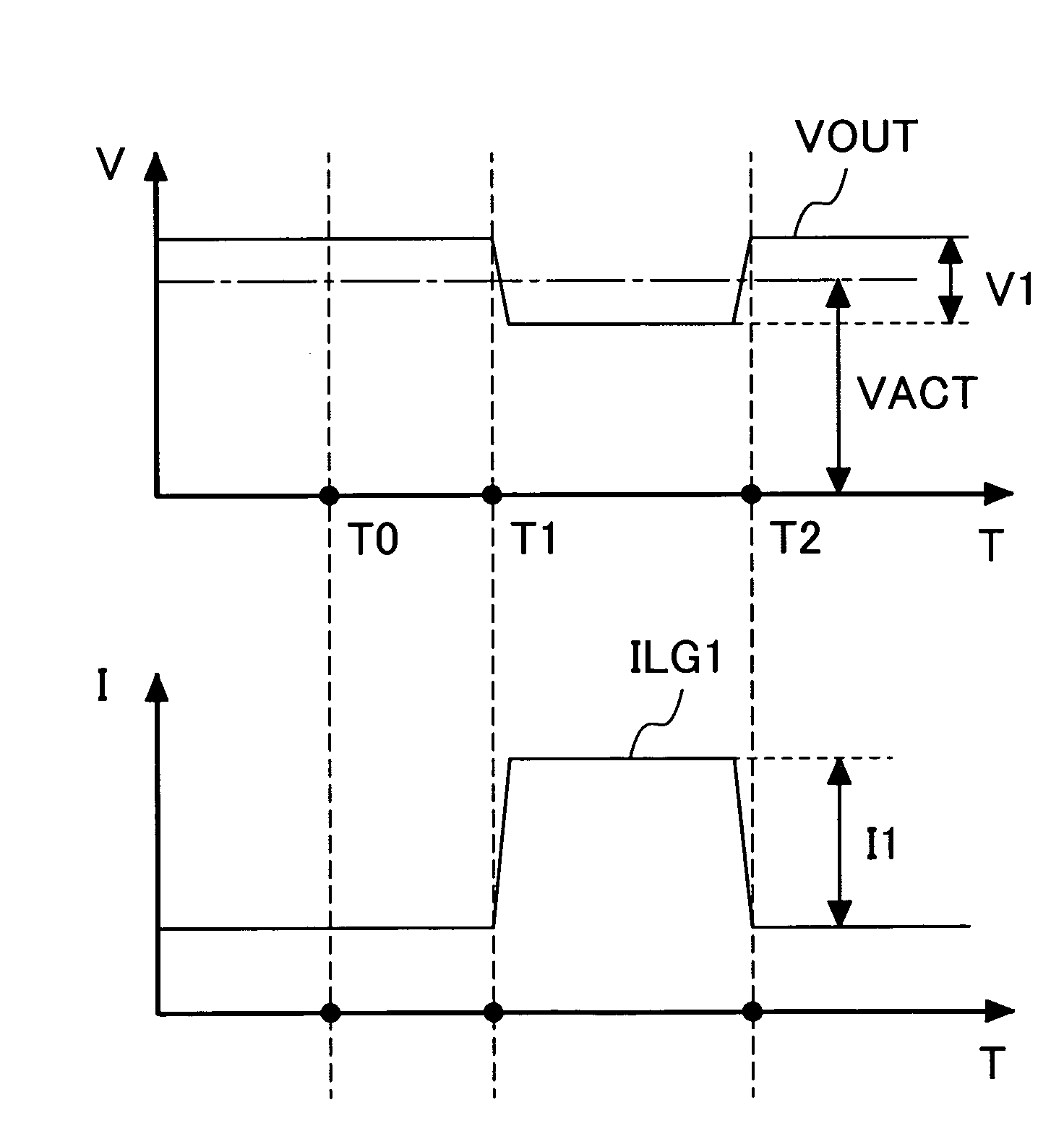
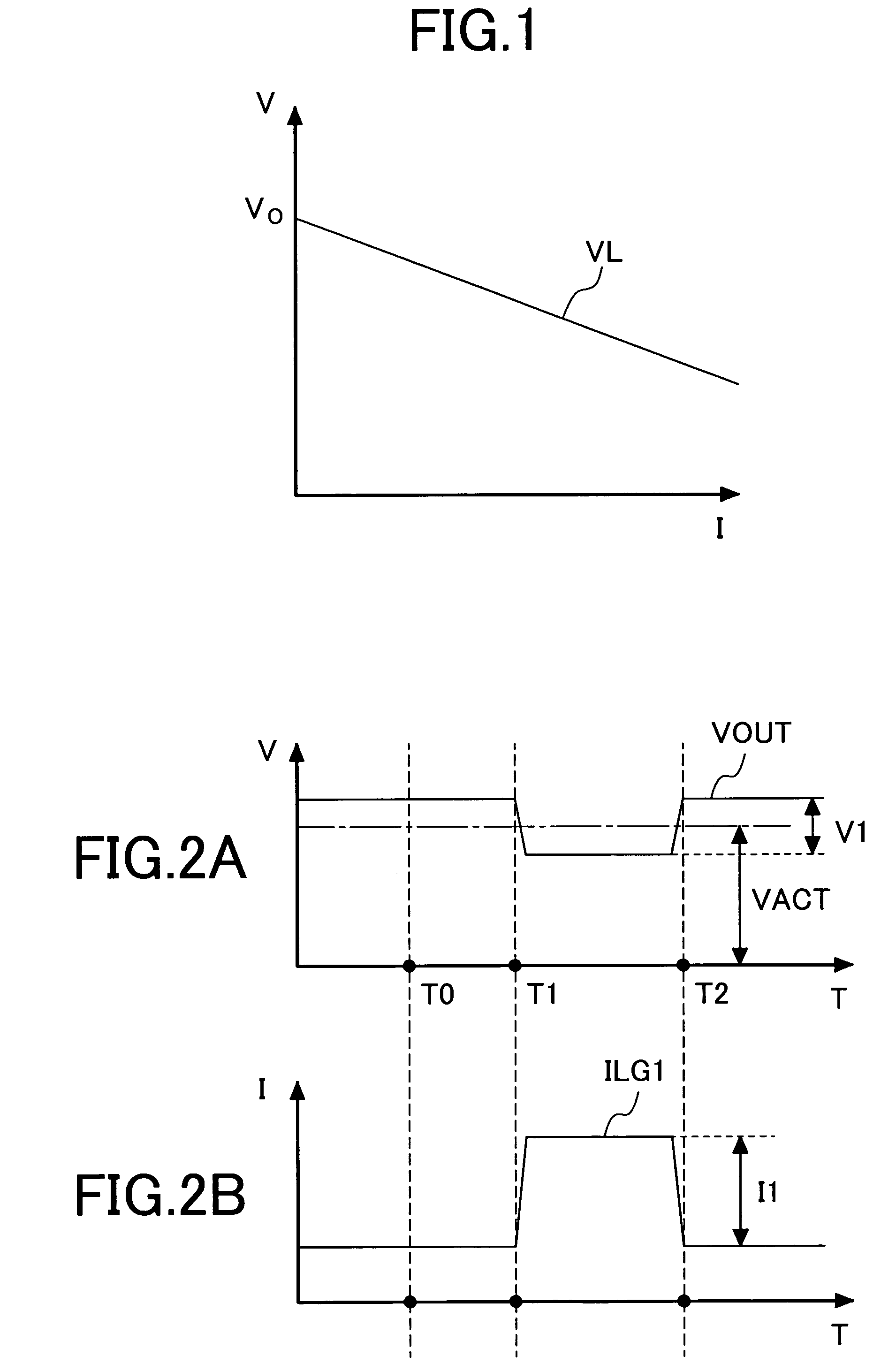
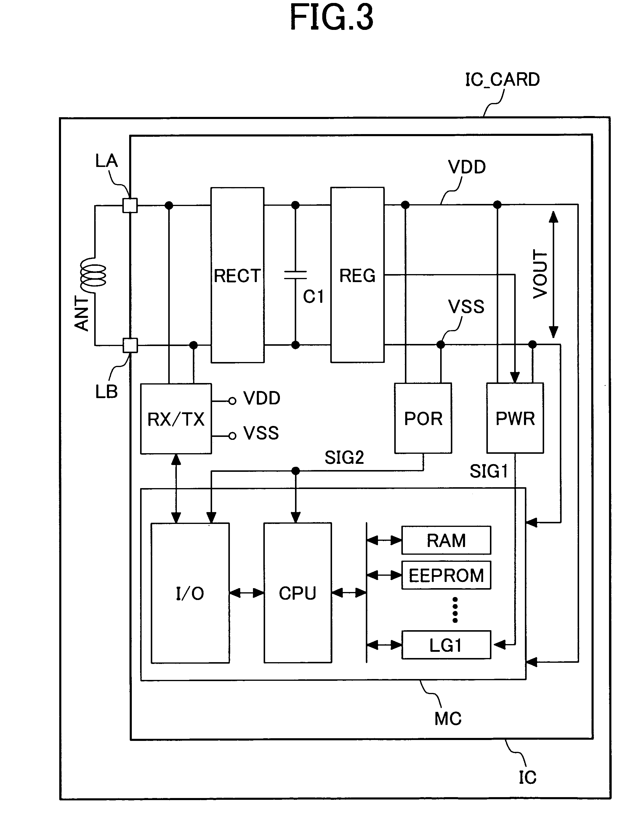
[0021]FIG. 3 is a block diagram of an embodiment of a semiconductor integrated circuit device provided with an operating current detector circuit according to the present invention and a contactless IC card having the semiconductor integrated circuit device mounted therein. The signal and power outputted in the form of electromagnetic wave from an interrogator (not shown) through an antenna are received by an antenna ANT incorporated in an IC card IC_CARD. Typically, the antenna ANT is an antenna coil formed of wound spiral of wire of a printed circuit board. The semiconductor integrated circuit IC is mounted on the printed circuit board having this antenna ANT formed thereon. This printed circuit board is molded with resin to form the IC card. Typically, the present invention is applied to a contactless IC card which does not have electrodes for I / O to and from outside on its surface. Of course, it is also possible to apply the present invention to a dual-type IC ...

second embodiment

(Second Embodiment)

[0041]FIG. 7 is a circuit diagram showing another embodiment of the voltage controlling circuit REG and the operating current detector circuit PWR in FIG. 4. The voltage comparator circuit VCC in FIG. 7 has the same configuration as that in FIG. 4. Meanwhile, the voltage controlling current source VCCS differs in that the drain of the NMOS M11 is directly connected to VDD.

[0042]The operating current detector circuit PWR in FIG. 7 is composed of the circuit described below. More specifically, the NMOS M12 whose gate terminal is connected to the output terminal of the operational amplifier circuit A01 is connected between the connection node N12 and the reference potential VSS. In this case, the size of the NMOS M12 is N times as large as that of the NMOS transistor M11. The reference current source IREF11 is connected between the power supply potential VDD and the connection node N12, the connection node 12 is connected to the input terminal of the inverter INV11, ...

third embodiment

(Third Embodiment)

[0047]FIG. 8 is a circuit diagram showing another embodiment of the operating current detector circuit PWR mounted in a semiconductor integrated circuit device according to the present invention. In this embodiment, a modification example of the operating current detector circuit PWR shown in FIG. 7 is described.

[0048]The operating current detector circuit PWR in FIG. 8 is composed of a circuit described below. That is, the NMOS M21 whose gate terminal is connected to the output terminal of the operational amplifier circuit A01 is connected between the connection node N21 and the reference potential VSS. The reference current source IREF 21 is connected between the power supply potential VDD and the connection node N21, an input terminal of the low pass filter LPF composed of the resistor R21 and the capacitor C11 is connected to the connection node N21, the PMOS M22 whose gate terminal is connected to the output terminal of the low pass filter LPF is connected bet...


PUM


Abstract

In an IC card in which an internal circuit is operated by an internal power supply formed from alternate current from outside received by an antenna, the voltage of the internal power supply sometimes changes due to the operation of the internal circuit. Therefore, the voltage controlling circuit of the present invention includes a voltage controlling current source, and when the internal circuit is not operated and the current higher than a predetermined current is detected in the voltage controlling current source, an operating current detector circuit outputs an enable signal. When the internal circuit is operated in response to the enable signal, the current consumed in the internal circuit is subtracted from the current passing through the voltage controlling current source. Consequently, the current change in the entire internal power supply can be prevented, and the output voltage of the internal power supply can be kept constant.

Description

TECHNICAL FIELD OF THE INVENTION[0001]The present invention relates to a semiconductor device. More particularly, the present invention relates to a circuit for detecting whether or not power for operating a signal processing unit mounted in a semiconductor integrated circuit device for contactless IC card is present.BACKGROUND OF THE INVENTION[0002]The documents cited in this specification are as follows, and these documents are cited based on their document numbers. Document 1: Japanese Patent Application Laid-Open No. 10-207580. The document 1 describes a voltage-monitoring type power on reset circuit (for example, FIG. 2) mounted in a contactless IC card which is operated by the operating voltage formed by rectifying the alternate current (AC) supplied from outside. The signal outputted from this power on reset circuit is used for the reset of the microcomputer mounted in the IC card.[0003]The so-called contactless IC card in which a semiconductor integrated circuit device and a...

Claims


Application Information

Patent Timeline
Patent Type & Authority Patents(United States)
IPC IPC(8): G06K19/06G05F3/24G06K19/07G11C5/14H01L21/8238H03K17/22
CPCG06K19/0707G11C5/142G06K19/0723G06K19/0712
Inventor WATANABE, KAZUKITSUNODA, HISATAKAYAMAMOTO, NORIHISAMATSUSHITA, KAZUHIRO
Owner RENESAS ELECTRONICS CORP
Why Eureka
Try Eureka