

Semiconductor device
A semiconductor and device technology, which is applied in the field of semiconductor devices including electrically rewritable non-volatile memory, can solve the problems of increasing memory cells and difficulty in maintaining a constant programming voltage level.
- Summary
- Abstract
- Description
- Claims
- Application Information
AI Technical Summary
Problems solved by technology
Method used
Image

Examples
no. 1 example
[0032] [Overall structure of semiconductor device]
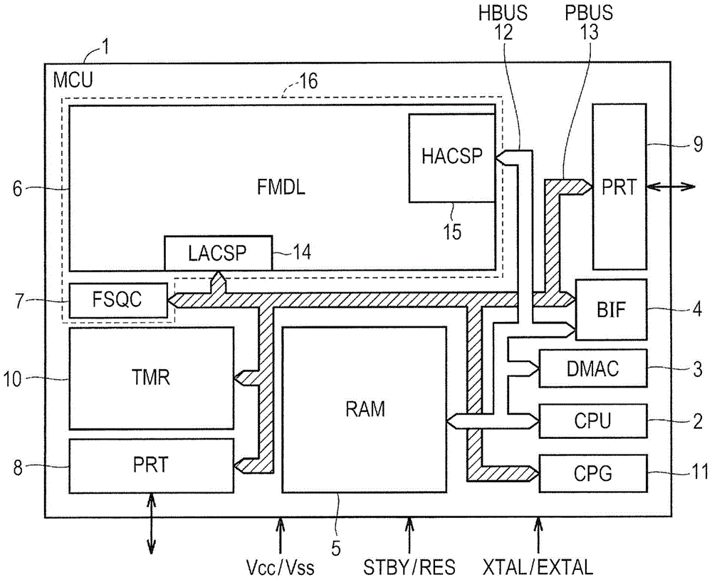
[0033] figure 1 is a block diagram showing the configuration of the semiconductor device according to the first embodiment. figure 1 The configuration of a microcomputer (MCU) 1 incorporating a flash memory module 16 as one example of a semiconductor device is shown. The boosted voltage supply circuit 400 described in this embodiment is also applicable to a semiconductor device in which only the flash memory module 16 is mounted on a single silicon substrate.
[0034] refer to figure 1 The microcomputer 1 is formed on a single semiconductor chip made of, for example, single crystal silicon using CMOS (Complementary Metal Oxide Semiconductor) integrated circuit manufacturing technology or the like.
[0035] Such as figure 1 As shown in , the microcomputer 1 includes a central processing unit (CPU) 2, a random access memory (RAM) 5, and a flash memory module (FMDL) 6. The central processing unit 2 includes an instruction ...
no. 2 example
[0126] [Structure of Boost Voltage Supply Circuit]
[0127] Figure 11 is a schematic diagram showing the configuration of a boosted voltage supply circuit 400A in the semiconductor device according to the second embodiment. Figure 11 The boost voltage supply circuit 400A is Image 6 A modified example of the boosted voltage supply circuit 400 in , and includes a control current generating circuit 105 instead of according to Image 6 The control current generation circuit 104 is shown in the first embodiment.
[0128] More specifically, refer to Figure 11 , the control current generating circuit 105 includes NMOS transistors Q405, Q406. The NMOS transistor Q405 is diode-coupled, and is coupled between the drain (node N401) of the PMOS transistor Q402 and the ground node GND. NMOS transistor Q406 is coupled between voltage dividing node 610 (coupling node between resistance elements R401 and R402 ) of voltage dividing circuit 102 and ground node GND (ie coupled in para...
no. 3 example
[0153] [Structure of Boost Voltage Supply Circuit]
[0154] Figure 14 is a schematic diagram showing the configuration of the boosted voltage supply circuit 500 in the semiconductor device according to the third embodiment. Figure 14 The boost voltage supply circuit 500 in the Image 6 A modified example of the boost voltage supply circuit 400 in FIG. More specifically, Figure 14 The boost voltage supply circuit 500 in the different Image 6 The boost voltage supply circuit 400 in FIG. 1 is that the boost voltage supply circuit 500 also includes a temperature-dependent current source 106 that increases the output current as the temperature increases.
[0155] refer to Figure 14 , the temperature-dependent current source 106 includes a constant voltage circuit 501, a resistance element R501, and NMOS transistors Q501, Q502. The constant voltage circuit 501 is configured with, for example, a BGR (Band Gap Reference) circuit, and outputs a constant voltage regardless of...
PUM
 Abstract
Description
Claims
Application Information