

Varactor with improved tuning range
- Summary
- Abstract
- Description
- Claims
- Application Information
AI Technical Summary
Problems solved by technology
Method used
Image

Examples
Embodiment Construction
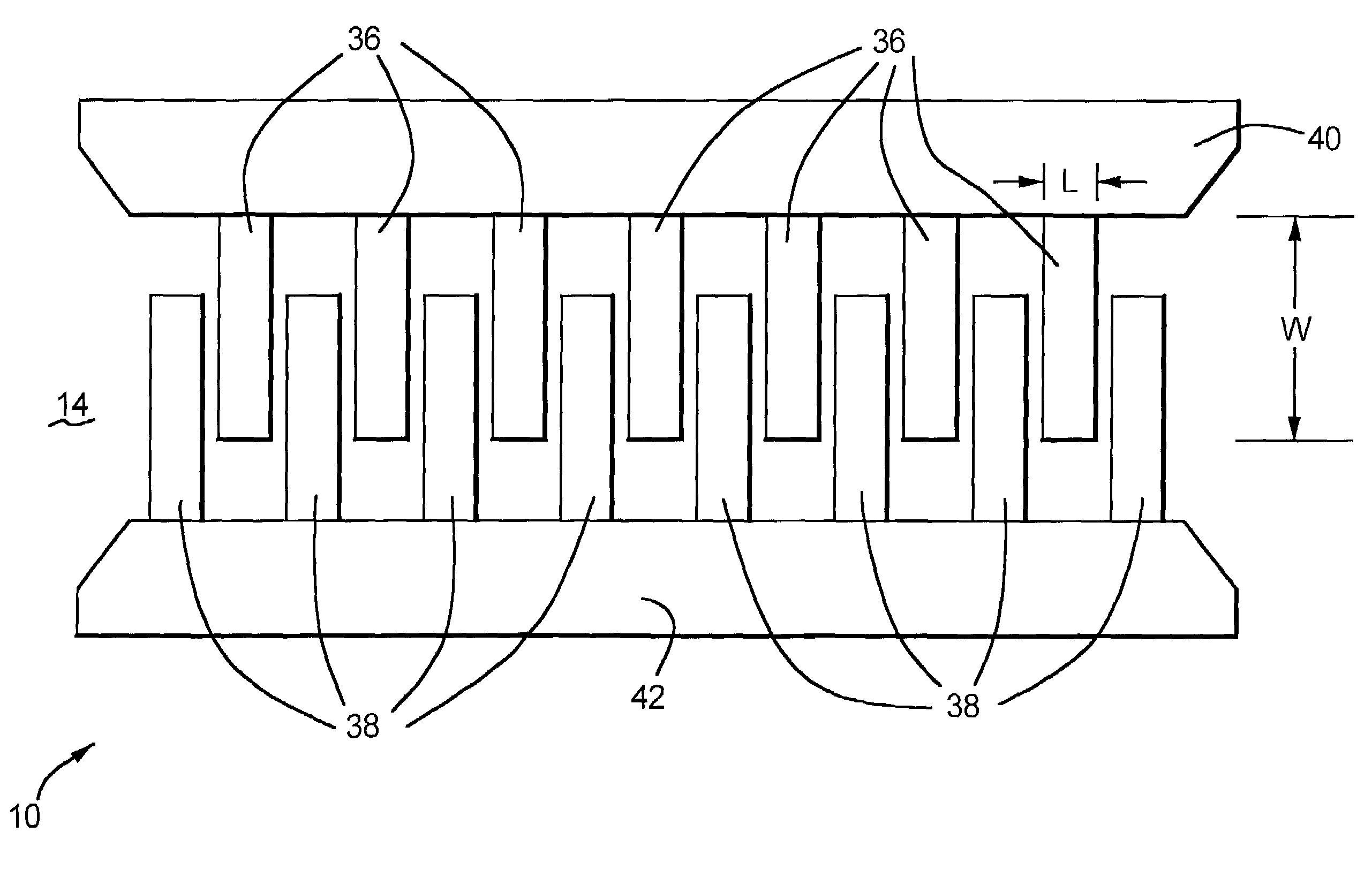
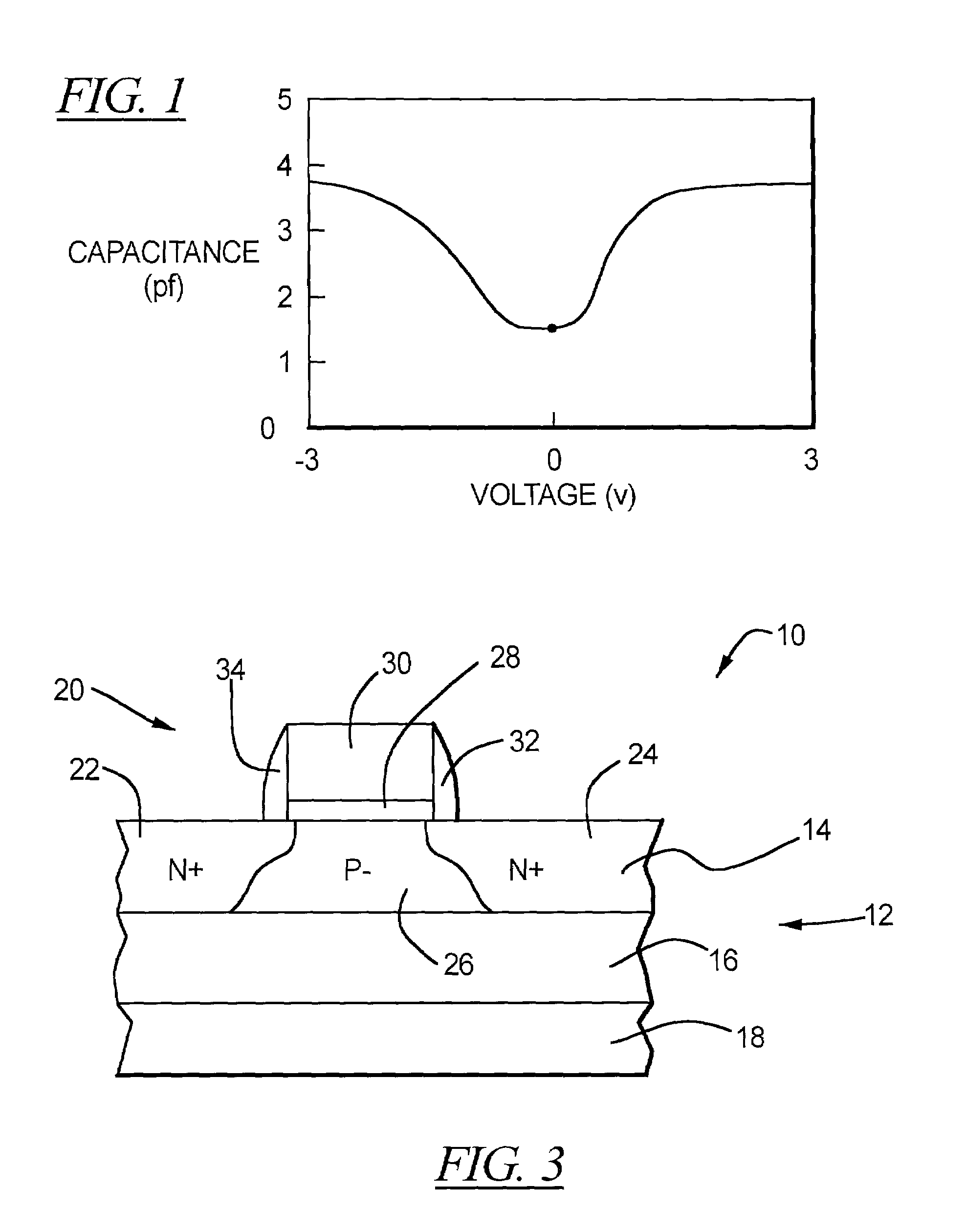
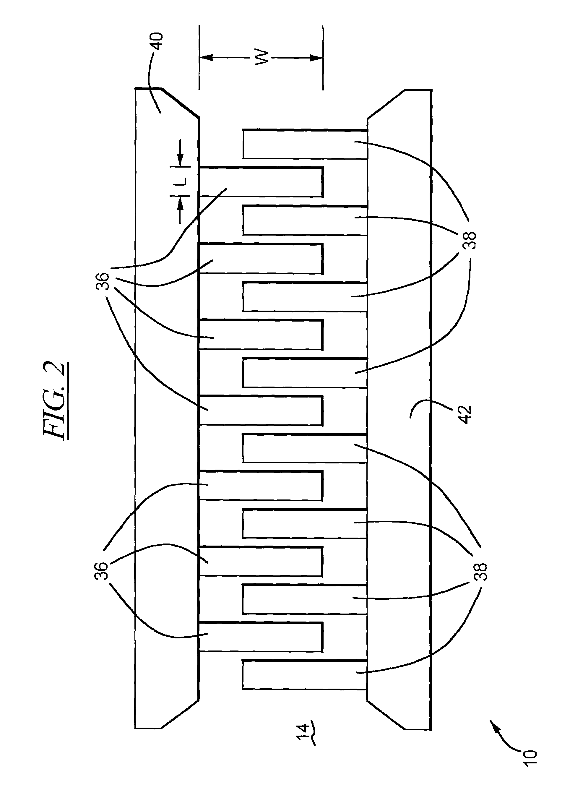
[0017]As shown in FIGS. 2 and 3, a varactor 10 is formed on a silicon-on-insulation (SOI) structure 12 having a silicon layer 14 formed over an insulation layer 16. The insulation layer 16 may be formed of an oxide such as SiO2 and, as shown in FIG. 3, is formed over a handle wafer 18. Silicon having a high resistivity may be used for the handle wafer 18. A plurality of MOS transistors is used to construct the varactor 10. A cross-sectional side view of one such transistor 20 is shown in FIG. 3.
[0018]As shown in FIG. 3, the silicon layer 14 is doped to form two N+ regions 22 and 24, one of which forms a source and the other of which forms a drain of the transistor 20. The silicon in the silicon layer 14 between the N+ regions 22 and 24 is suitably doped in order to form a P− well 26. A gate oxide 28 is provided over the P− well 26, and a polysilicon gate 30 is provided over the gate oxide 28. The gate oxide 28 and the polysilicon gate 30 are defined by suitable dielectric spacers 32...
PUM
 Abstract
Description
Claims
Application Information