Inverted light emitting diode on conductive substrate

a technology of light-emitting diodes and conductive substrates, which is applied in the direction of semiconductor/solid-state device manufacturing, semiconductor devices, electrical apparatus, etc., can solve the problems of preventing most researchers from producing commercially successful devices, obtaining the necessary pure single crystal of silicon carbide, and the typical epitaxial or implanted layer. , to achieve the effect of increasing current spreading, increasing conductivity, and increasing brightness

Active Publication Date: 2007-01-30
CREELED INC
View PDF25 Cites 53 Cited by
  • Summary
  • Abstract
  • Description
  • Claims
  • Application Information

AI Technical Summary

Benefits of technology

[0019]Preferred embodiments of the invention include a LED structure that will emit light within the ultraviolet to green portion of the spectrum and that will do so while maximizing the use of n-type material to take advantage of its higher conductivity, greater current spreading, and resulting increased brightness in an LED.

Problems solved by technology

Because the wavelength of light is inversely proportional to its frequency, and its frequency is directly proportional to the corresponding energy transition, certain wavelengths of light cannot be obtained in materials that have relatively narrow bandgaps.
Nevertheless, the difficulties of working with silicon carbide have precluded most researchers from producing commercially successful devices from it.
As a result, and as well known to those familiar with crystal growth techniques of semiconductors and other materials, obtaining the necessary pure single crystals of silicon carbide, and the typical epitaxial or implanted layers that are generally desired or required in many semiconductor device structures, has long been a difficult task.
Silicon carbide, however, is an “indirect” semiconductor, meaning that when a radiative recombination occurs in SiC, some of the energy is released as a phonon rather than a photon, thus reducing the overall efficiency of the process.
For the time being, however, Group III nitride materials are not commonly available in bulk or substrate form.
Sapphire cannot be conductively doped, however, and thus cannot form the basis of “vertical” devices, i.e. those in which ohmic contacts can be conveniently placed at opposite ends of the device.
Furthermore, producing successful ohmic contacts to p-type Group III nitride layers has often required a relatively high temperature anneal of the layer and the contact.
Thus, an n-p-n structure would prevent current flow in either the forward or reverse direction, thereby rendering the device inoperative.
Although these issues have been addressed to some extent in silicon carbide devices (e.g. U.S. Pat. No. 5,338,944; commonly assigned herewith and incorporated entirely herein by reference), they have not yet been addressed for the Group III-nitride devices.
However, the device described in the '944 patent has a silicon carbide active region, which, as is discussed above, has a low efficiency of emission due to its indirect bandgap.
In addition, Moreover, the device described in the '944 patent requires the formation of an ohmic contact to n-type silicon carbide after epitaxial deposition of the active layer, which typically requires additional dopant implantation and / or annealing steps.

Method used


Image

  • Inverted light emitting diode on conductive substrate
  • Inverted light emitting diode on conductive substrate
  • Inverted light emitting diode on conductive substrate

Examples


Embodiment Construction

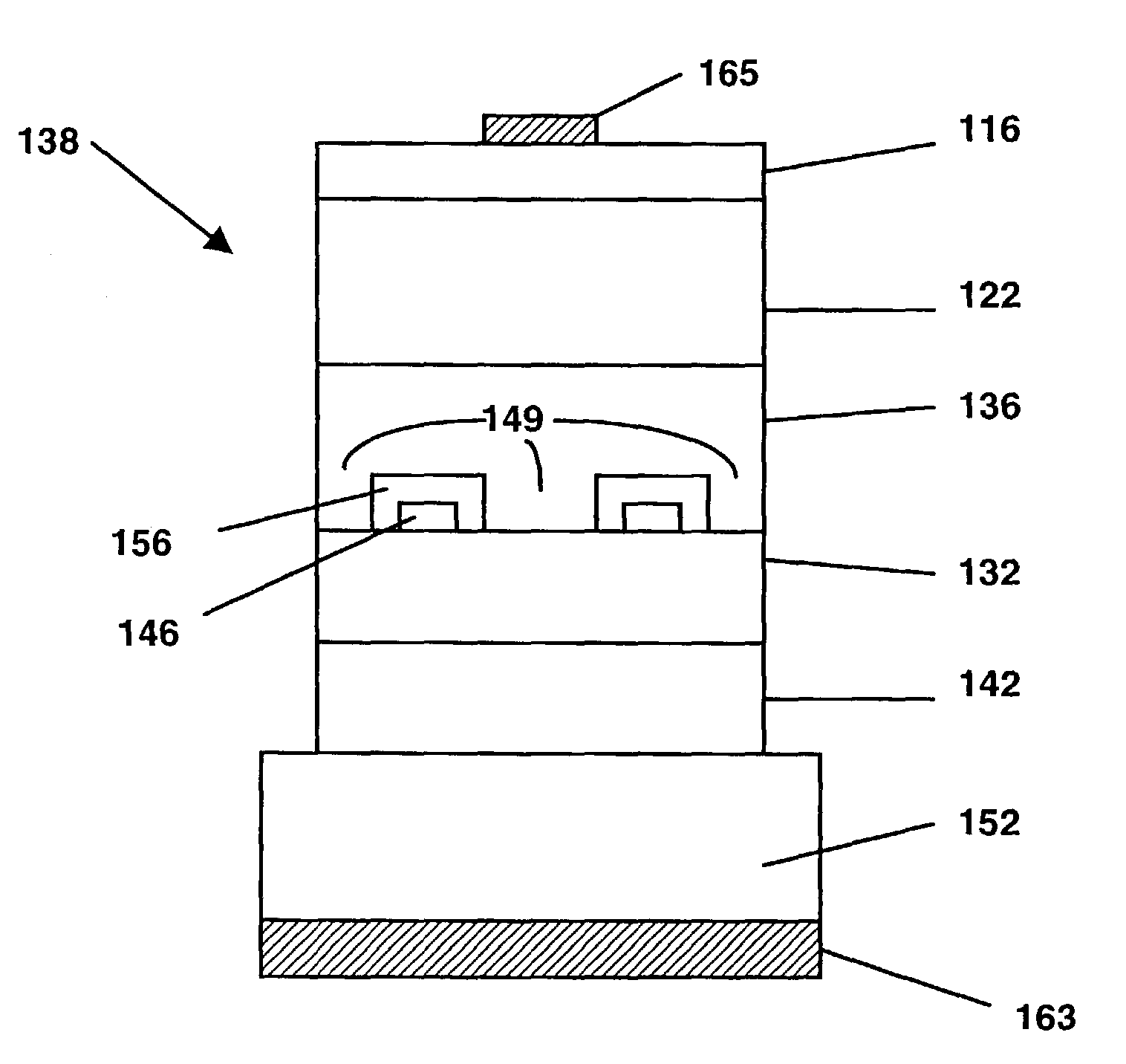
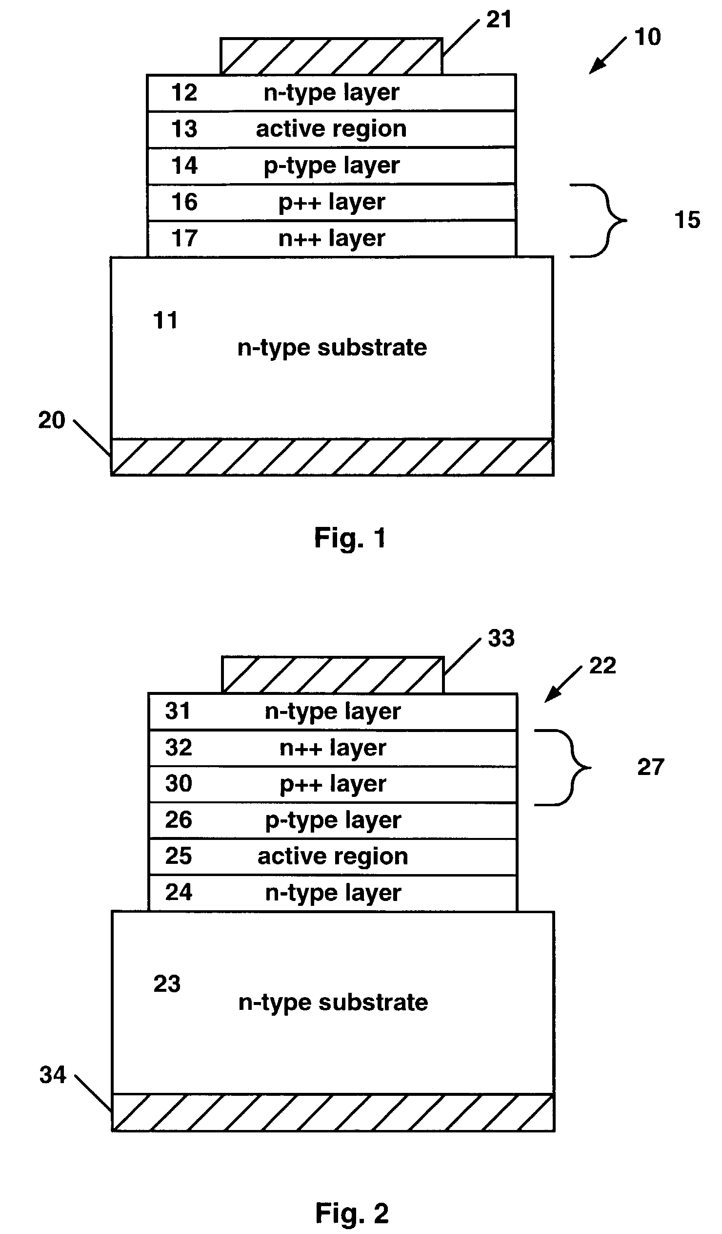
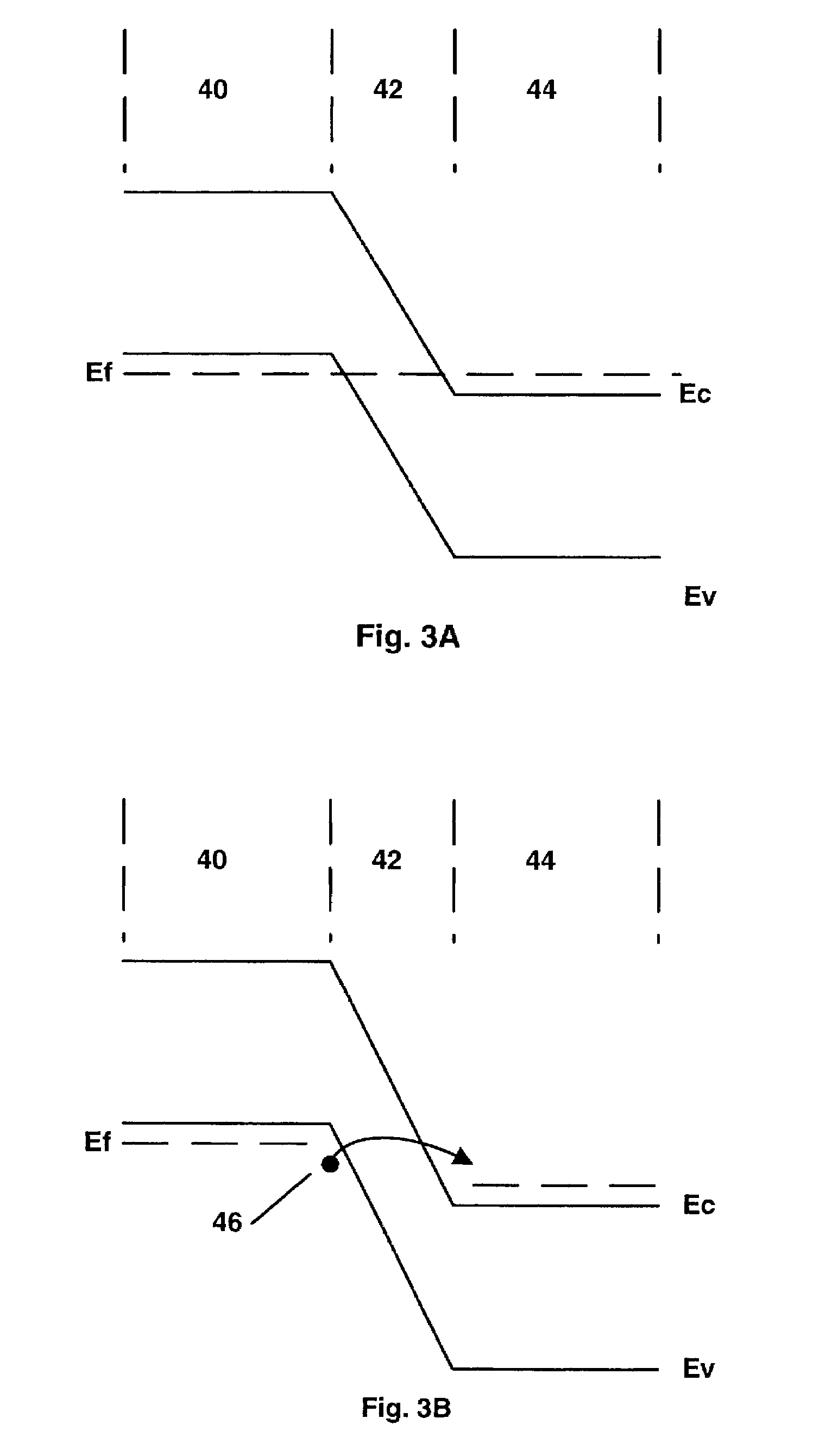
[0029]The present invention may be illustrated by reference to the embodiments set forth herein. According to a first embodiment of the invention, a light emitting diode broadly designated at 10 is illustrated in FIG. 1. As will be described herein, by various combinations and doping of Group III nitride materials in the active layer, such a diode can be tuned to emit in many portions of the physical spectrum, but for a number of purposes, the diode 10 is often most valuable in its capability to light in the ultraviolet (UV) to green portion of the electromagnetic spectrum. p As illustrated in FIG. 1, the diode 10 is formed on an n-type layer or substrate 11 which is preferably silicon carbide, but which may be bulk gallium nitride or any other suitable conductive n-type substrate. In preferred embodiments, the substrate is a single crystal silicon carbide substrate having a polytype selected from the group consisting of 3C, 4H, 6H and 15R. In a most preferred embodiment, the substr...


PUM


Abstract

An electronic device includes a conductive n-type substrate, a Group III nitride active region, an n-type Group III-nitride layer in vertical relationship to the substrate and the active layer, at least one p-type layer, and means for providing a non-rectifying conductive path between the p-type layer and the n-type layer or the substrate. The non-rectifying conduction means may include a degenerate junction structure or a patterned metal layer.

Description

RELATED APPLICATIONS[0001]This application incorporates entirely by reference co-pending and commonly-assigned applications Ser. No. 09 / 706,057 (Group III Nitride Light Emitting Devices with Gallium-Free Layers), and Ser. No. 09 / 760,635 (Group III Nitride LED with Undoped Cladding Layer).FIELD OF THE INVENTION[0002]The present invention relates to semiconductor devices formed in wide bandgap semiconductor materials, and in particular relates to light-emitting devices with improved efficiency and brightness that combine a Group III nitride active layer with an n-type substrate and that emit visible light in the UV to green portion of the spectrum.BACKGROUND OF THE INVENTION[0003]A light-emitting diode (LED) is a widely used semiconductor device whose main characteristic is that it will emit energy in the form of light, usually within the visible spectrum, when a current flows through the device. The basic mechanisms by which light-emitting diodes operate are well understood in this a...

Claims


Application Information

Patent Timeline
Patent Type & Authority Patents(United States)
IPC IPC(8): H01L29/15H01L33/00H01L33/04H01L33/14
CPCH01L33/0004H01L33/145H01L33/04
Inventor EDMOND, JOHN ADAMDOVERSPIKE, KATHLEEN MARIEBERGMANN, MICHAEL JOHNKONG, HUA-SHUANG
Owner CREELED INC
Why Eureka
Try Eureka