Arrangement with p-doped and n-doped semiconductor layers and method for producing the same

a technology of ndoped and p-doped semiconductors, applied in the direction of coatings, solid-state devices, chemical vapor deposition coatings, etc., can solve the problem of providing voltage limitation for both polarities

Inactive Publication Date: 2007-01-30
ROBERT BOSCH GMBH
View PDF10 Cites 0 Cited by
  • Summary
  • Abstract
  • Description
  • Claims
  • Application Information

AI Technical Summary

Benefits of technology

[0007]In an example embodiment of the present invention a plurality of transitions between p-doped semiconductor layers and n-doped semiconductor layers are present; and characteristic voltages additively make up a breakdown voltage of the entire arrangement. Through the present invention it is no longer necessary to use two separate components to bring about voltage limitation for both polarities of the voltage. Instead, a single arrangement having multiple transitions between p-doped semiconductor layers and n-doped semiconductor layers provides voltage limitation for both polarities. Since the characteristic voltages of the transitions at which the trans

Problems solved by technology

Instead, a single arrangement having multiple transitions between p-doped semiconductor

Method used


Image

  • Arrangement with p-doped and n-doped semiconductor layers and method for producing the same
  • Arrangement with p-doped and n-doped semiconductor layers and method for producing the same
  • Arrangement with p-doped and n-doped semiconductor layers and method for producing the same

Examples


Embodiment Construction

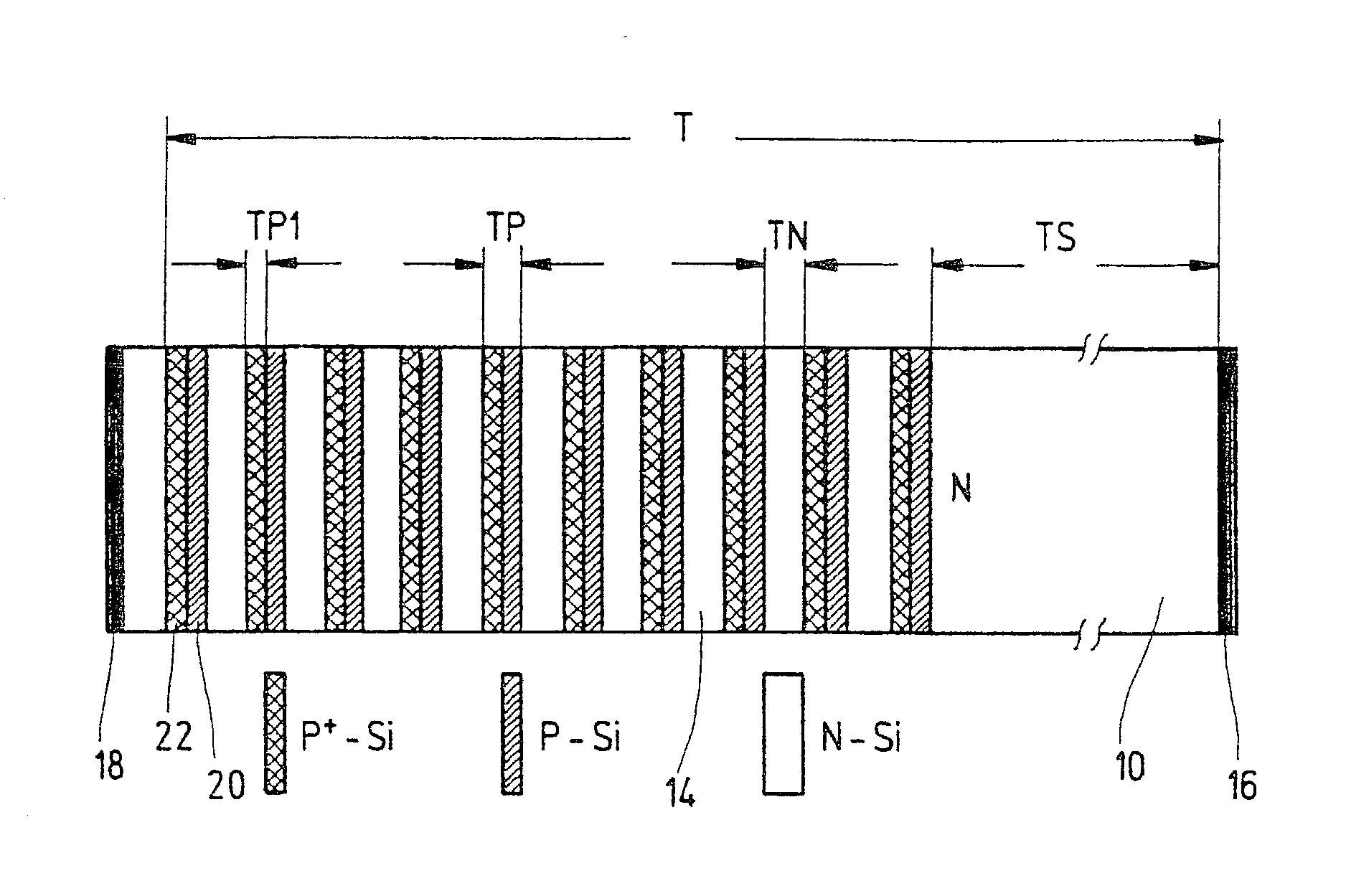
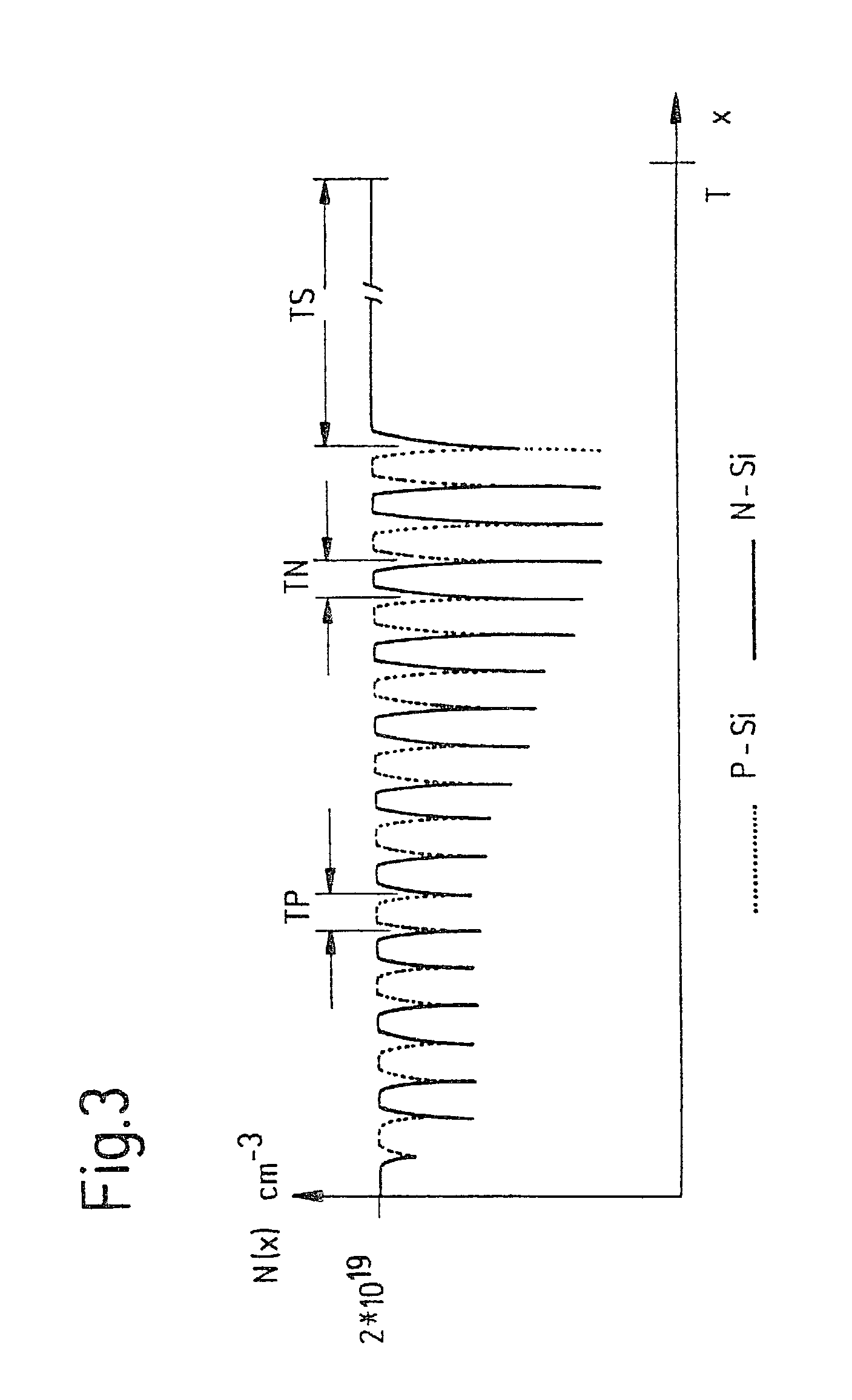
[0038]FIG. 1 schematically shows a cross section of an arrangement according to the present invention. A plurality of p-doped semiconductor layers 12 and n-doped semiconductor layers 14 are arranged on an n-doped silicon substrate 10. A plurality of semiconductor transitions are present between p-doped semiconductor layers 12 and n-doped semiconductor layers 14. P-doped semiconductor layers 12 have a thickness TP, while n-doped semiconductor layers have a thickness TN. In the present case, thicknesses TP and TN are approximately identical and are approximately 4 μm. The substrate has a thickness TS of approx. 525 μm in the present example. Since a total of ten p-doped semiconductor layers and ten n-doped semiconductor layers 14 are arranged on substrate 10, the total thickness T of the arrangement resulting from these data is 605 μm. In the present example, silicon is selected as the semiconductor. Located on n-doped substrate 10 and the uppermost semiconductor layer, which in the p...


PUM

PropertyMeasurementUnit
Lengthaaaaaaaaaa
Thicknessaaaaaaaaaa
Concentrationaaaaaaaaaa

Abstract

An arrangement having p-doped semiconductor layers and n-doped semiconductor layers which exhibits transitions between the p-doped semiconductor layers and n-doped semiconductor layers, the transitions displaying a Zener breakdown upon application of a voltage characteristic of a transition, a plurality of transitions between p-doped semiconductor layers and n-doped semiconductor layers being present, and the characteristic voltages additively make up the breakdown voltage of the entire arrangement. Also described is a method for manufacturing the arrangement.

Description

FIELD OF THE INVENTION[0001]The present invention relates to an arrangement having p-doped and n-doped semiconductor layers which exhibits transitions between the p-doped semiconductor layers and n-doped semiconductor layers, the transitions displaying a Zener breakdown upon application of a voltage characteristic of a transition. The present invention further concerns a method for manufacturing the arrangement according to the present invention.BACKGROUND OF THE INVENTION[0002]The use of semiconductor components to limit voltages is known. Zener diodes (Z diodes), in particular, are used for this purpose. If Zener diodes are operated in the blocking or reverse direction, they display a pronounced breakdown behavior at comparatively low breakdown voltages. The value of the breakdown voltage of a diode depends substantially on the doping concentration of the semiconductor material. In highly doped diodes, a very narrow barrier layer forms, so that high electrical field strengths abov...

Claims


Application Information

Patent Timeline
IPC IPC(8): H01L29/866H01L27/08
CPCH01L29/866H01L27/0814
Inventor SPITZ, RICHARDGOERLACH, ALFRED
Owner ROBERT BOSCH GMBH
Why Eureka
Try Eureka