Methods for forming semiconductor devices including thermal processing

a technology of thermal processing and semiconductor devices, applied in the direction of capacitors, semiconductor devices, electrical equipment, etc., can solve the problems of leakage current, increased dielectric constant, and unsuitable polysilicon layer for capacitor electrodes, so as to reduce interface stress, reduce interface stress, and reduce interface stress

Inactive Publication Date: 2007-02-06
SAMSUNG ELECTRONICS CO LTD
View PDF9 Cites 10 Cited by
  • Summary
  • Abstract
  • Description
  • Claims
  • Application Information

AI Technical Summary

Benefits of technology

[0013]Performing the thermal process may include performing the thermal process on the second conductive layer and the dielectric layer after removing portions of the second conductive layer and the dielectric layer. Moreover, the thermal process may reduce an interface stress between the second conductive layer and the dielectric layer and / or cure the dielectric layer. In addition, the thermal process may be performed on the second conductive layer and the dielectric layer while maintaining the dielectric layer in a substantially amorphous state during and after the thermal process.
[0014]According to additional embodiments of the present invention, methods for fabricating a semiconductor memory device may include forming a first conductive layer for a first electrode on a semiconductor substrate, forming a tantalum oxide layer on the first conductive layer, and forming a second conductive layer for a second electrode on the tantalum oxide layer. Portions of the second conductive layer and the tantalum oxide layer can be removed, and a thermal process may be performed to reduce an interface stress between the second conductive layer and the tantalum oxide layer and to cure the tantalum oxide layer. Moreover, the tantalum oxide layer can be maintained in a substantially amorphous state during and after the thermal process.
[0015]According to still additional embodiments of the present invention, methods for fabricating a semiconductor memory device may include forming a first conductive layer for a first electrode on a semiconductor substrate, forming a tantalum oxide layer on the first conductive layer, and forming a second conductive layer for a second electrode on the tantalum oxide layer. Portions of the second conductive layer and the tantalum oxide layer can be removed, and a thermal process can be performed to reduce interface stress between the second conductive layer and the tantalum oxide layer and to crystallize the tantalum oxide layer.
[0016]According to still additional embodiments of the present invention, methods for fabricating a semiconductor memory device may include forming a first conductive layer for a first electrode on a semiconductor substrate, forming a seed layer on the first conductive layer, and crystallizing the seed layer. A tantalum oxide layer can be formed on the crystallized seed layer, and a second conductive layer for a second electrode can be formed on the tantalum oxide layer. Portions of the second conductive layer and the tantalum oxide layer can be removed, and a thermal process can be performed to reduce an interface stress between the second conductive layer and the tantalum oxide layer and to cure the tantalum oxide layer.

Problems solved by technology

When the thickness of a dielectric layer is reduced, leakage currents may occur due to tunneling effects.
Accordingly, when a material having high electric constant, such as Ta2O5 or BST ((Ba,Sr)TiO3), is used as a dielectric material, a polysilicon layer may be unsuitable for use as a capacitor electrode.
On the other hand, when the tantalum oxide layer 30 is crystallized, the dielectric constant may increase but leakage current characteristics may deteriorate.
However, the thermal processes after depositing the dielectric layer and etching the conductive layer for the upper electrode may complicate the conventional method for manufacturing an MIM capacitor.
In other words, since a wafer may need to be transferred for each thermal process, the conventional method may require an increased amount of time, and contaminants may remain on the wafer.

Method used


Image

  • Methods for forming semiconductor devices including thermal processing
  • Methods for forming semiconductor devices including thermal processing
  • Methods for forming semiconductor devices including thermal processing

Examples


Embodiment Construction

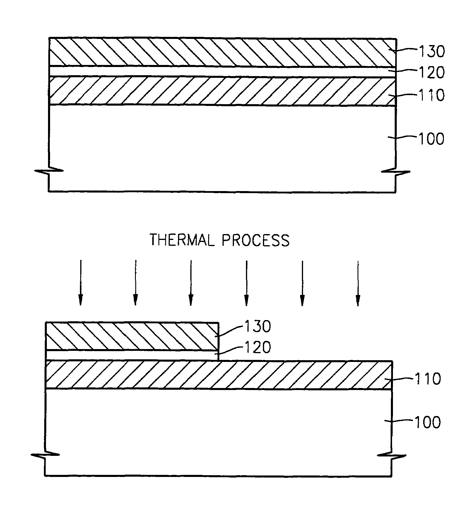
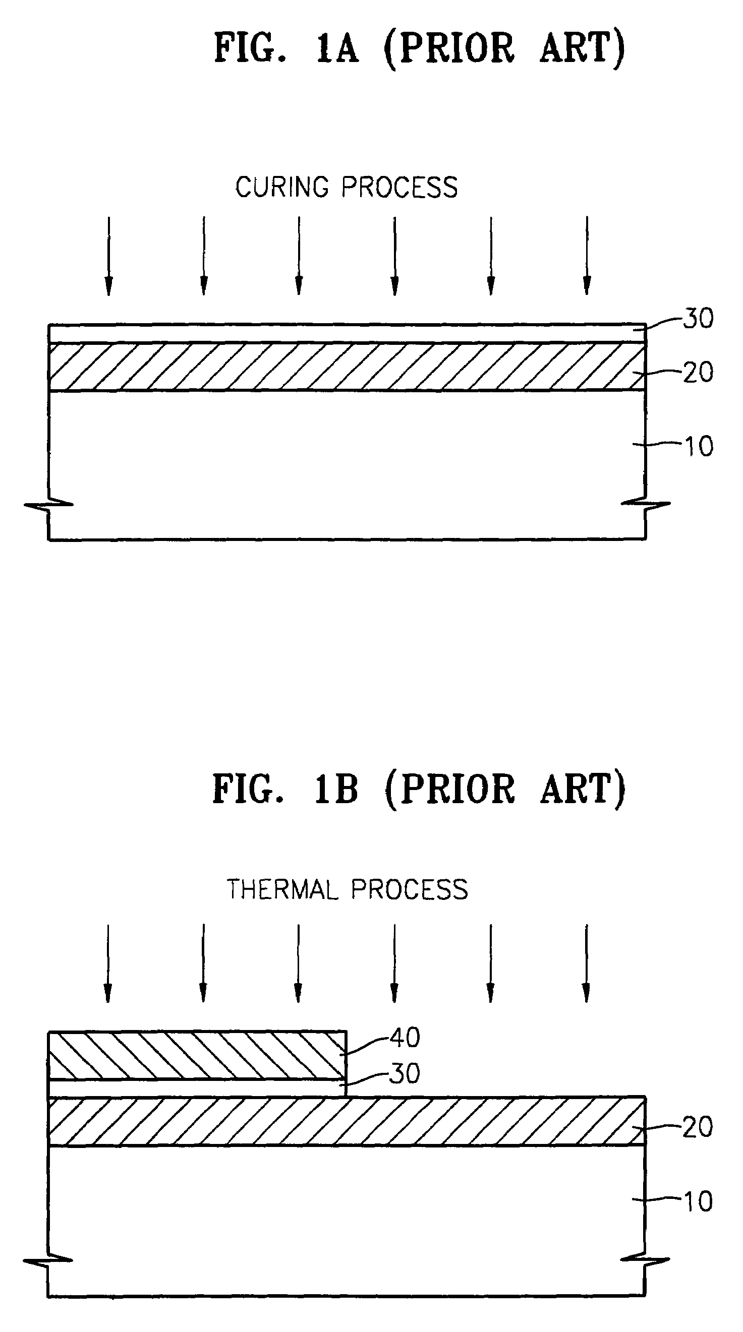
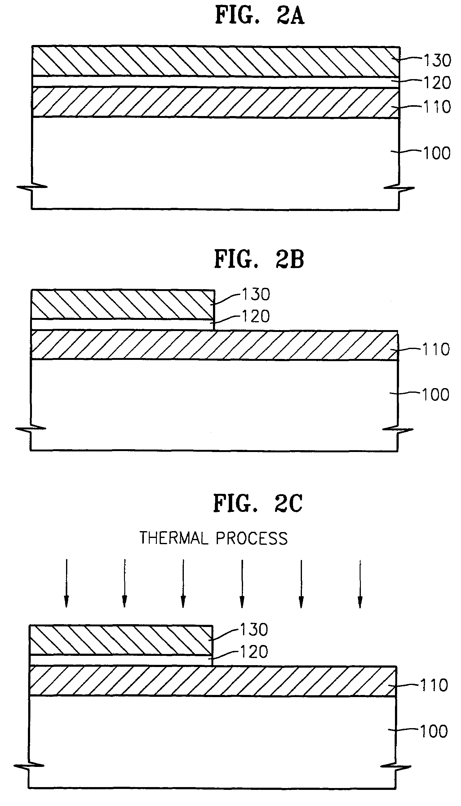
[0027]The present invention will now be described more fully with reference to the accompanying drawings, in which preferred embodiments of the invention are shown. This invention may, however, be embodied in many different forms and should not be construed as being limited to the embodiments set forth herein; rather, these embodiments are provided so that this disclosure will be thorough and complete, and will fully convey the concept of the invention to those skilled in the art. In the drawings, the size and the thickness of layers and regions are exaggerated for clarity. It will also be understood that when a layer is referred to as being on another layer or substrate, it can be directly on the other layer or substrate, or intervening layers may also be present.

[0028]FIGS. 2A through 2C are cross-sectional views illustrating methods for manufacturing metal-insulator-metal (MIM) capacitors according to embodiments of the present invention. Referring to FIG. 2A, a conductive layer ...


PUM

PropertyMeasurementUnit
temperatureaaaaaaaaaa

Abstract

Methods for fabricating semiconductor memory devices may include forming a first conductive layer for a first electrode on a semiconductor substrate, forming a dielectric layer on the first conductive layer, and forming a second conductive layer for a second electrode on the dielectric layer. Portions of the second conductive layer and the dielectric layer can be removed, and a thermal process can be performed on the second conductive layer and the dielectric layer. The thermal process can reduce interface stress between the second conductive layer and the dielectric layer and/or cure the dielectric layer. In addition, the dielectric layer may be maintained in an amorphous state during and after the thermal process.

Description

RELATED APPLICATIONS[0001]This application claims the benefit of priority from Korean Patent Application No. 2002-73820, filed on Nov. 26, 2002 in the Korean Intellectual Property Office, the disclosure of which is incorporated herein in its entirety by reference.FIELD OF THE INVENTION[0002]The present invention relates to methods for manufacturing semiconductor devices, and more particularly, to methods for manufacturing capacitors.BACKGROUND OF THE INVENTION[0003]As the integration of semiconductor devices has increased, the area occupied by individual devices on a semiconductor substrate (chip) has been reduced. Information storage capacitors for DRAM devices, however, may need to maintain a same or increased capacitance within a reduced area. Accordingly, various methods have been developed to provide increased capacitor electrode surface areas. For example, capacitors having lower electrodes with three-dimensional shapes such as cylindrical shapes or fin shapes have been provid...

Claims


Application Information

Patent Timeline
Patent Type & Authority Patents(United States)
IPC IPC(8): H01L21/20H01L27/04H01L21/02H01L21/314
CPCH01L28/65H01L28/40H01L27/04
Inventor CHOI, JAE-HYOUNGKIM, WAN-DONYOO, CHA-YOUNGCHUNG, SUK-JIN
Owner SAMSUNG ELECTRONICS CO LTD
Why Eureka
Try Eureka