System and method of design for testability

a technology of testability and system, applied in the direction of error detection/correction, cad circuit design, instruments, etc., can solve the problems of hardware function description degrade, controllability and observability analysis is relatively difficult to achieve, hardware function description timing characteristics may degrad

Inactive Publication Date: 2007-02-06
RICOH KK
View PDF8 Cites 7 Cited by
  • Summary
  • Abstract
  • Description
  • Claims
  • Application Information

AI Technical Summary

Benefits of technology

[0018]Accordingly, it is an object of the present disclosure to provide an improved system and method for implementing design for testability, capable of executing controllability and observability analysis at the stage of hardware function description independent of architecture, having m

Problems solved by technology

In the known LogicBIST, however, there gives rise to several drawbacks, which follow.(1) Since the controllability and observability can be verified only after the fault simulation, a certain time period is required for CAD tool execution with respect to several steps such as logic synthesis, scan path, LogicBIST controller insertion, and fault simulator execution.(2) Since the analysis of the controllability and observability is verified by the net list at the gate level, the analysis is relatively hard to achie

Method used


Image

  • System and method of design for testability
  • System and method of design for testability
  • System and method of design for testability

Examples


example 1

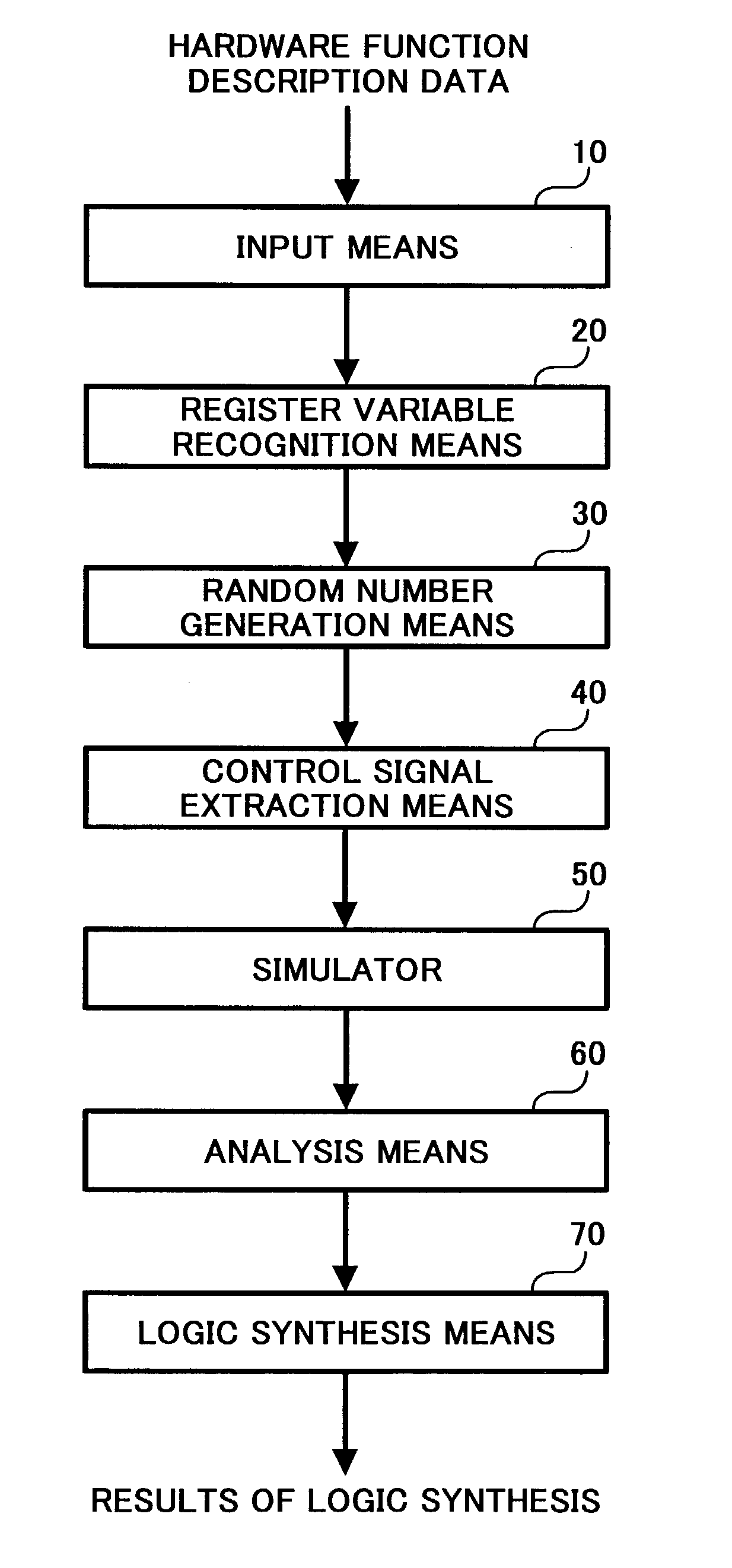
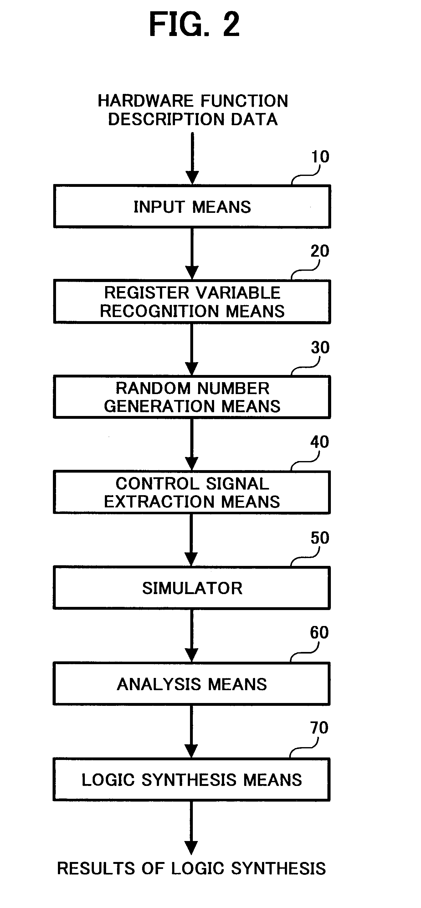
[0097]FIG. 2 is a block diagram illustrating the functional structure of the system for implementing design for testability (DFT system) according to one embodiment disclosed herein.

[0098]Referring to FIG. 2, the functional structure includes an input means 10, register variable recognition means 20, random number generation means 30, control signal extraction means 40, simulator 50, analysis means 60, and logic synthesis means 70.

[0099]The input means 10 is adapted to read the hardware function description independent of architecture by input unit 1 to be stored temporarily in the storage unit 5 for use in the following process.

[0100]The hardware function description independent of architecture is herein made in terms of the description language such as, for example, VHDL (very high speed IC (VHSIC) hardware description language (HDL)) and Verilog-HDL, which are standardized by IEEE.

[0101]The input means 10 may alternatively be adapted to read out the hardware function description ...

example 2

[0139]FIG. 9 is a block diagram illustrating the functional structure of a further DFT system according to another embodiment disclosed herein.

[0140]Referring to FIG. 9, the functional structure of Example 2 includes an input means 10, register variable recognition means 20, random number generation means 30, control signal extraction means 40, simulator 50, analysis means 60, and function description data generation means 80.

[0141]Like reference numerals in FIG. 9 designate the components each having the same or corresponding function of those in FIG. 2 (Example 1), in which the description on these components is herein abbreviated. The description on other components is included as follows.

[0142]The function description data generation means 80 functions to generate function description data with test points inserted with respect to the control signals having low toggle rates among the control signals extracted from the control signal extraction means 40.

[0143]For example, functio...

example 3

[0146]FIG. 10 is a block diagram illustrating the functional structure of a DFT system according to still another embodiment disclosed herein.

[0147]Referring to FIG. 10, the functional structure of Example 3 includes an input means 10, register variable recognition means 20, random number generation means 30, control signal extraction means 40, simulator 50, analysis means 60, and test point insertion means 90.

[0148]Like reference numerals in FIG. 10 designate the components each having the same or corresponding function of those in FIG. 2 (Example 1), in which the description on these components is herein abbreviated. The description on other components is included as follows.

[0149]The test point insertion means 90 instructs to read the results obtained by logic synthesis of the function description data input by the input means 10, and, based on logical interconnection information included in the thus read logic synthesis results, to insert test points corresponding to the control...


PUM


Abstract

A system and a method for implementing design for testability is disclosed, in that the method includes the steps of inputting function description data for defining hardware functions represented in the form independent of architecture; recognizing register variables inferable by memory elements, which are contained in the function description data; simulating events induced by affixing random numbers to the register variables; extracting control signals contained in the function description data as extracted control signals; analyzing the results of the simulation with respect to the extracted control signals; inserting test points for control signals having low toggle rates among the extracted control signals; and executing logic synthesis on the control signals having low toggle rates including the test points.

Description

BACKGROUND[0001]1. Field[0002]This patent specification relates generally to a system and a method for implementing design for testability, and more particularly to such method for identifying the portion with reduced controllability and observability at the stage of hardware function description independent of architecture utilizing test inputs from a pseudorandom number generator in the course of testing large scale integrated devices by means of Logic BIST.[0003]2. Discussion of the Background[0004]An integration of semiconductor devices advances toward higher in density and more complex in operation, the period of time for preparing test patterns for integrated circuits is also increasing to such an extent as to exceed their designing time in some cases.[0005]In the process for fabricating large scale integrated devices, therefore, the method of ‘Design for Testability (DFT)’ has been increasingly indispensable, in that the means for facilitating the generation and execution of ...

Claims


Application Information

Patent Timeline
IPC IPC(8): G06F17/50H01L21/82H01L21/822H01L27/04
CPCG06F17/5045G06F17/5022G06F30/30G06F30/33G06F30/3308
Inventor YAMADA, TAKAMITSU
Owner RICOH KK
Why Eureka
Try Eureka