
Electronic device, dielectric ceramic composition and the production method

a technology of dielectric ceramics and electronic devices, applied in ceramics, fixed capacitors, electrical equipment, etc., can solve the problems of frequent short-circuit defects, high cost of precious metals such as platinum and palladium, and achieve excellent high temperature load lifetime, high reliability, and finer appearance.

Active Publication Date: 2007-02-13
TDK CORPARATION
View PDF9 Cites 10 Cited by
  • Summary
  • Abstract
  • Description
  • Claims
  • Application Information

AI Technical Summary

Benefits of technology

The present invention provides a production method for a dielectric ceramic composition that has good electric and temperature characteristics, even when used in a thin, multilayer ceramic capacitor. The composition includes a main component ingredient and a subcomponent ingredient. The subcomponent ingredient contains specific amounts of oxides of Mg, Mn, Cr, and R, among others. The main component ingredient is barium titanate ingredient powder with a specific ratio of A site components and B site components and a specific surface area. The dielectric ceramic composition produced by this method has small particle sizes and can be made thinner, more compact, and multilayered. The invention also provides an electronic device that includes a dielectric layer made of the dielectric ceramic composition.

Problems solved by technology

Therefore, costly precious metals, such as platinum and palladium, had to be used as the material composing the internal electrode layer.
However, when a dielectric layer is made thinner, there arises a disadvantage that a short-circuiting defective is frequently caused.

Method used


Image

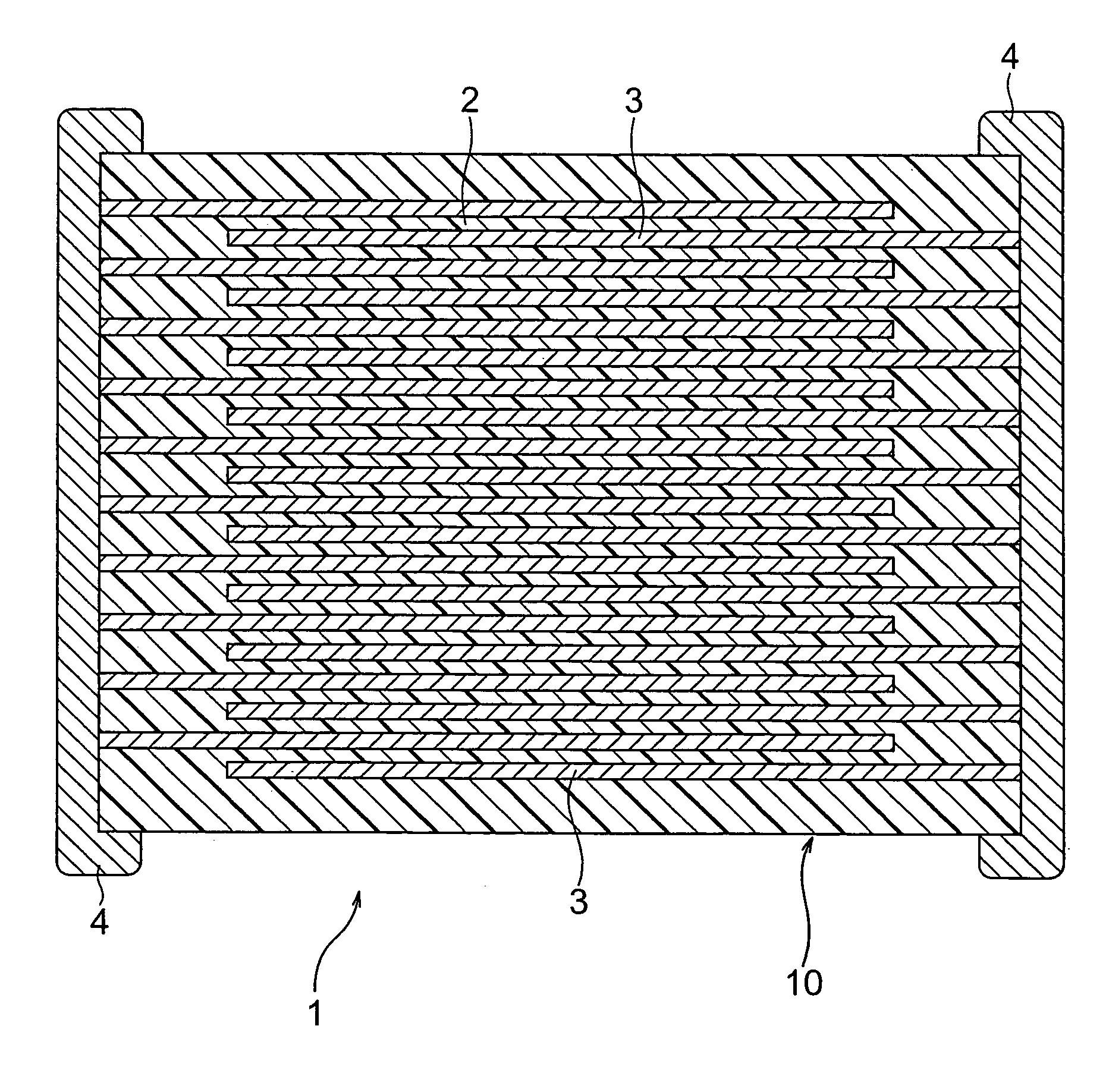
  • Electronic device, dielectric ceramic composition and the production method
  • Electronic device, dielectric ceramic composition and the production method
  • Electronic device, dielectric ceramic composition and the production method

Examples


example 1

[0103]As a main component material, barium titanate ingredient powder having the specific surface area and A / B as shown in Table 1 below was prepared.

[0104]The specific surface area of the barium titanate ingredient powder was measured by the nitrogen absorption method (BET method). Also, the A / B of the, barium titanate ingredient powder was obtained by measuring the weight ratio (abundance ratio) of a composition existing in the powder including impurities by using a fluorescence X-ray analysis device (3550 made by Rigaku Corporation) and converting the weight ratio to the mole ratio. Namely, number of mole of each element is calculated from the weight ratio of the each composition obtained by the measurement result, and the A / B value was calculated by dividing the number of mole of Ba, Sr and Ca as elements included in the A site by the number of moles of Ti and Zr as elements included in the B site.

[0105]Note that as a detailed result of fluorescent X-ray analysis, for example, t...

example 2

[0140]Except that the subcomponents expressed in Table 2 were used as the subcomponent ingredients, samples 19 to 26 of a multilayer ceramic capacitor were produced in the same way as in the example 1, and a thickness of the dielectric layer, short-circuiting defective rate, specific permittivity, high temperature load lifetime and temperature characteristic of electrostatic capacity were measured in the same way as in the example 1. Also, the specific surface area and the A / B value of barium titanate ingredient powder used in producing the capacitor samples 19 to 26 were also measured in the same way as in the example 1. The powder characteristic of barium titanate material, kinds and adding quantities of subcomponents, and chip characteristic and electric characteristics of the capacitor samples are shown in Table 2 and Table 3.

[0141]

TABLE 2PowderCharacteristicof BariumTitanateRaw MaterialSpecificSubcomponentSurfaceAddingAddingAddingAddingAddingSampleAreaCom-QuantityCom-QuantityCo...


PUM

PropertyMeasurementUnit
specific surface areaaaaaaaaaaa
thicknessaaaaaaaaaa
thicknessaaaaaaaaaa

Abstract

A production method of a dielectric ceramic composition having a step of firing dielectric material including a main component ingredient and a subcomponent ingredient, wherein said main component ingredient before firing is barium titanate ingredient powder having the perovskite type crystal structure expressed by ABO3, and a ingredient powder having a ratio A / B of A site components and B site components of 1.006≦A / B≦1.035 and the specific surface area of 8 to 50 m2 / g is used. According to the invention, a dielectric ceramic composition having preferable electric characteristics and temperature characteristic can be provided even in the case of being composed of fine particle and a capacitor made to be a thin layer.

Description

BACKGROUND OF THE INVENTION[0001]1. Field of the Invention[0002]The present invention relates to a production method of a dielectric ceramic composition used as a dielectric layer of, for example, a multiplayer ceramic capacitor, a dielectric ceramic composition obtained by the production method, and an electronic device using the dielectric ceramic composition as a dielectric layer.[0003]2. Description of the Related Art[0004]A multilayer ceramic capacitor as an example of electronic devices is produced, for example, by alternately stacking ceramic green sheets made by a predetermined dielectric ceramic composition and internal electrode layers of a predetermined pattern and unifying the result, and cofiring a thus obtained green chip. It is necessary that a material which does not react with a ceramic dielectric is selected for the internal electrode layer of the multilayer ceramic capacitor so as to be unified with the ceramic dielectric by firing. Therefore, costly precious meta...

Claims


Application Information

Patent Timeline
Patent Type & Authority Patents(United States)
IPC IPC(8): C04B35/468C04B35/46H01B3/12H01G4/12
CPCH01G4/1227C04B35/64C04B35/63B32B2311/22C04B2235/3206C04B2235/3213C04B2235/3215C04B2235/3224C04B2235/3225C04B2235/3236C04B2235/3239C04B2235/3241C04B2235/3256C04B2235/3258C04B2235/3262C04B2235/3267C04B2235/3436C04B2235/3454C04B2235/5409C04B2235/5445C04B2235/6582C04B2235/6588C04B2235/662C04B2235/72C04B2235/79C04B2237/346C04B2237/405C04B35/468
Inventor UMEDA, YUJISATO, AKIRA
Owner TDK CORPARATION
Learn More