High frequency chip packages with connecting elements

a technology of connecting elements and chips, applied in the direction of instruments, semiconductor/solid-state device details, radio-controlled devices, etc., can solve the problems of relatively large space, relatively simple routing on the connecting element, and large traces, so as to reduce the cost of the package, and reduce the connection impedance

Inactive Publication Date: 2007-02-13
TESSERA INC
View PDF109 Cites 317 Cited by
  • Summary
  • Abstract
  • Description
  • Claims
  • Application Information

AI Technical Summary

Benefits of technology

[0007]In a particularly preferred arrangement, the lower chip or chips are active semiconductor chips, most preferably RF chips such as RF power amplifier chips, whereas the upper chip or chips include one or more integrated passive chips. Such an integrated passive chip incorporates numerous passive components such as resistors, capacitors and inductors. In preferred structures according to this aspect of the invention, the terminals are disposed adjacent the periphery of the package, outside the area occupied by the lower semi-conductor chip or chips. Leads extend from these terminals upwardly to the connecting element. Thus, the connecting element carries signals horizontally in a plane above the lower chips and the leads carry the signals down to the terminals. Stated another way, the chip carrier handles the horizontal translation or “fan out” of signal traces from the contacts of the lower chips to the periphery of the connecting element. The upper chip or chips can be of any size. Typically, all of the passive components to be incorporated in an integra

Problems solved by technology

Moreover, the routing on the connecting element can be relatively un

Method used


Image

  • High frequency chip packages with connecting elements
  • High frequency chip packages with connecting elements
  • High frequency chip packages with connecting elements

Examples


Embodiment Construction

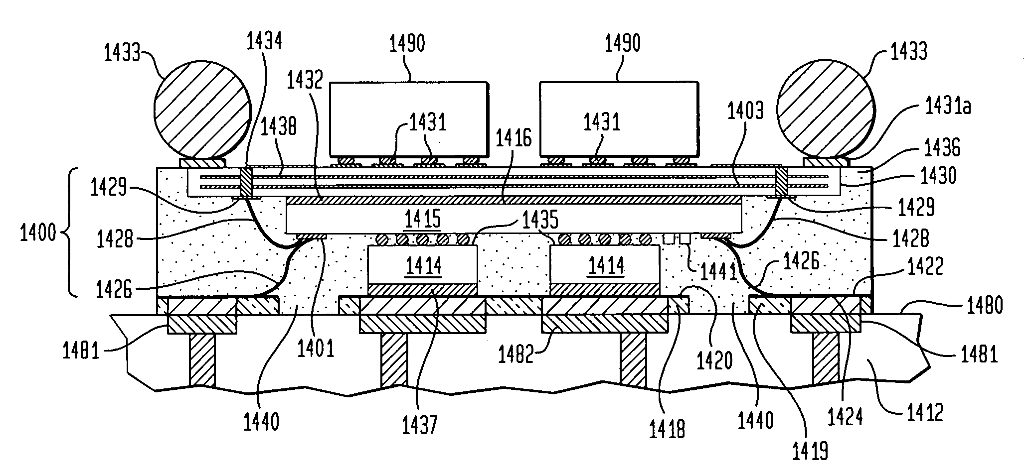
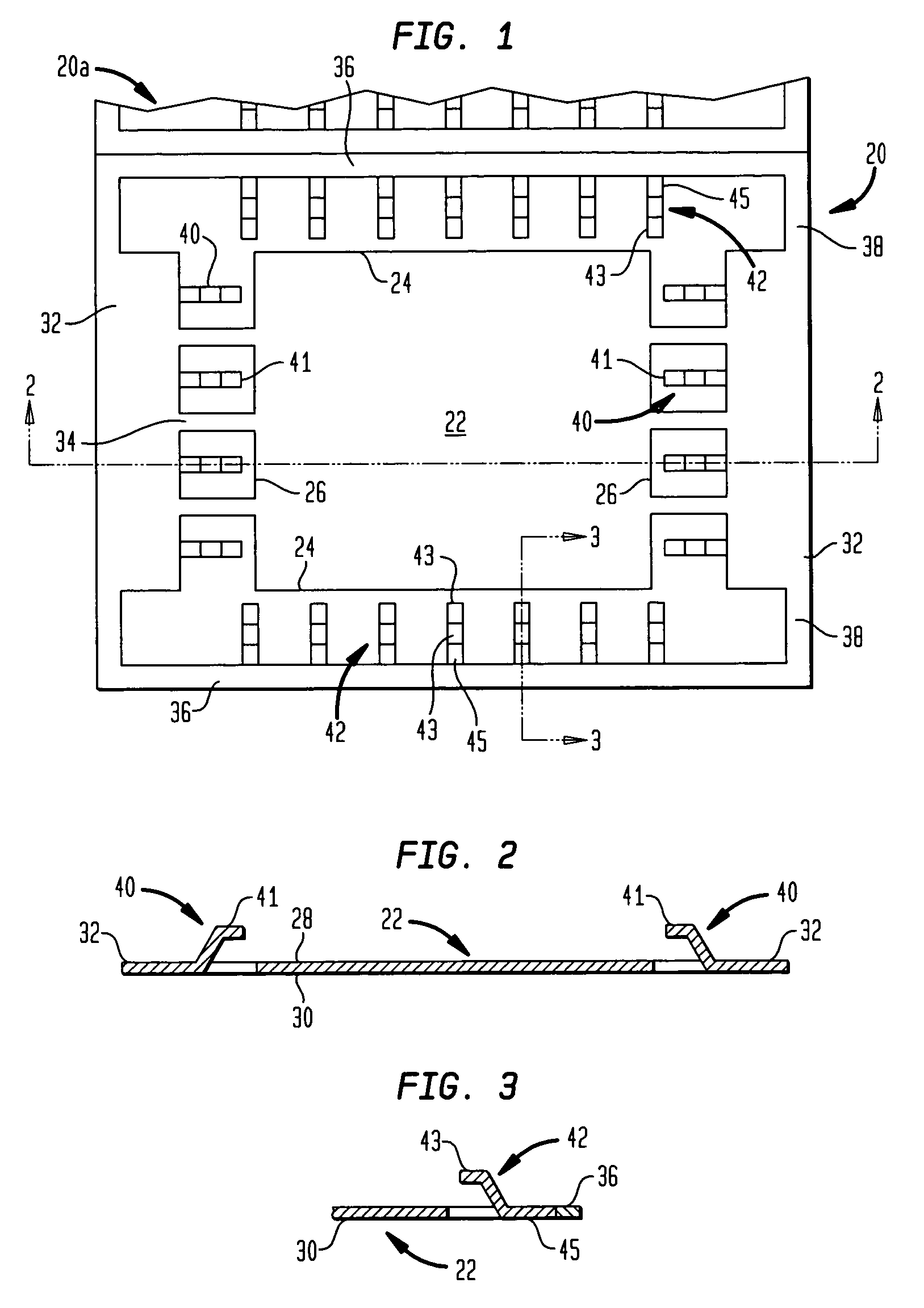
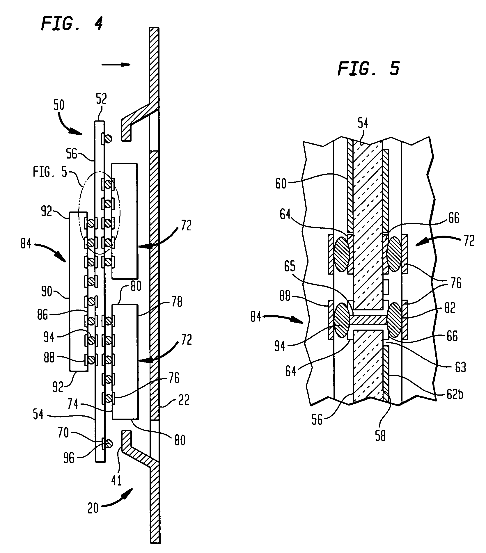
[0057]A lead frame 20 in accordance with one embodiment of the invention (FIG. 1) is formed as a unitary structure from a metal such as copper as, for example, copper on the order of 50–500 microns thick. The lead frame in accordance with this embodiment includes a central thermal conductor or plate 22 which is generally rectangular and has a pair of opposed edges 24 referred to herein as the active edges of the plate and a pair of additional opposed edges 26 referred to herein as the ground edges. The plate also has a top surface 28 and a bottom surface 30. The lead frame includes a pair of smaller rectangular plates referred to herein as ground buses 32 extending parallel to the ground edges 26 of the central plate. One or the other or both of the ground buses 32 can be used as ground connections in a completed assembly or as a power bus for supplying power. Hereinafter, the term ground bus shall refer to the structure, in which ever way it is used. The ground buses are connected ...


PUM


Abstract

A radio frequency chip package is formed by assembling a connecting element such as a circuit board or flexible circuit tape having chips thereon with a bottom plane element such as a lead frame incorporating a large thermally-conductive plate and leads projecting upwardly from the plane of the plate. The assembly step places the rear surfaces of the chips on the bottom side of the connecting element into proximity with the thermal conductor and joins the conductive traces on the connecting element with the leads. The resulting assembly is encapsulated, leaving terminals at the bottom ends of the leads exposed. The encapsulated assembly may be surface-mounted to a circuit board. The leads provide robust electrical connections between the connecting element and the circuit board.

Description

CROSS-REFERENCE TO RELATED APPLICATIONS[0001]The present application is a continuation-in-part of commonly assigned, co-pending international application PCT / US02 / 27509, filed Aug. 28, 2002, (hereinafter, the “'509 application”) which designates the United States. Said international application claims the benefit of U.S. Provisional Patent Application No. 60 / 315,408 filed Aug. 28, 2001. Said international application is also a continuation-in-part of U.S. patent application Ser. No. 10 / 210,160, filed Aug. 1, 2002 now U.S. Pat. No. 6,856,007, which application also claims the benefit of said U.S. Provisional Patent Application No. 60 / 315,408. The present application is also a continuation-in-part of said U.S. patent application Ser. No. 10 / 210,160, filed Aug. 1, 2002. The present application also claims the benefit of U.S. Provisional Patent Application No. 60 / 449,673 filed Feb. 25, 2003 and U.S. Provisional Patent Application No. 60 / 462,170 filed Apr. 11, 2003. The disclosures of al...

Claims


Application Information

Patent Timeline
IPC IPC(8): H01L27/148G06F21/00H01L23/24H01L23/31H01L23/367H01L23/433H01L23/498H01L23/552H01L23/64H01L25/065H03H9/05
CPCH01F17/0033H01L23/24H01L23/3107H01L23/3114H01L23/36H01L23/3675H01L23/4334H01L23/49531H01L23/49575H01L23/49822H01L23/49838H01L23/49861H01L23/5387H01L23/552H01L23/645H01L24/49H01L25/0652H01L25/0657H01L25/16H01L2223/6611H01L2224/16145H01L2224/48091H01L2224/4824H01L2224/4911H01L2224/73253H01L2224/73257H01L2224/73265H01L2225/0651H01L2225/06513H01L2225/06517H01L2225/0652H01L2225/06527H01L2225/06541H01L2225/06551H01L2225/06572H01L2225/06579H01L2225/06582H01L2924/01005H01L2924/01006H01L2924/01007H01L2924/01013H01L2924/01014H01L2924/01027H01L2924/01028H01L2924/01029H01L2924/01031H01L2924/01047H01L2924/0105H01L2924/01061H01L2924/01078H01L2924/01079H01L2924/01082H01L2924/01322H01L2924/01327H01L2924/15311H01L2924/1532H01L2924/15331H01L2924/16152H01L2924/19041H01L2924/19042H01L2924/19043H01L2924/19103H01L2924/19107H01L2924/3011H01L2924/3025H01L24/48H01L2924/01023H01L2924/01033H01L2924/01087H01L2924/014H01L2924/10253H01L2924/30107H01L2924/00014H01L2924/00H01L2224/85207H01L2924/01075H01L2924/12042H01L2924/15787H01L2924/30105H01L24/45H01L24/50H01L2224/05569H01L2224/05571H01L2224/05573H01L2224/16235H01L2224/32245H01L2224/45014H01L2224/451G06F21/10G06F2221/2129H01L2224/05599H01L2224/12105H01L2224/32145H01L2224/45099H01L2224/48145H01L2224/48225H01L2224/48227H01L2224/73204H01L2224/73207H01L2224/85399H01L2225/06568H01L2924/19011H01L2924/19104H01L2924/19105H03H9/0542H03H9/0547H03H9/1064H03H2009/0019H01L2224/45015H01L2924/207H01L2924/00012Y04S40/20
Inventor BEROZ, MASUDWARNER, MICHAELSMITH, LEEURBISH, GLENNKANG, TECK-GYUPARK, JAE M.KUBOTA, YOICHI
Owner TESSERA INC
Why Eureka
Try Eureka