Semiconductor device

Inactive Publication Date: 2007-02-13
RENESAS ELECTRONICS CORP
View PDF20 Cites 22 Cited by
  • Summary
  • Abstract
  • Description
  • Claims
  • Application Information

AI Technical Summary

Benefits of technology

[0014]An object of the invention is to hinder the latching-up that occurs when the supply voltage is applied to a CMOS

Problems solved by technology

When the supply voltage drops to 2 V or lower and when the threshold voltage VT is decreased to 0.5 V or lower correspondingly, however, the subthreshold leakage current increases, whereby the transistor cannot be cut off completely.
Consequently, the standby current of the LSI chip increases, which represents a bottleneck in the design of a system that includes a battery-powered CMOS LSI chip.
(1) An overcurrent flows because of latching-up when the power supply is turned on, and the wiring in the CMOS LSI chip may fuse, or the normal supply voltage may become inapplicable as the load exceeds the current capacitance of the power supply. This problem is caused because the layout and connections of the circuit are designed so that the substrate (well) and source of

Method used


Image

  • Semiconductor device
  • Semiconductor device
  • Semiconductor device

Examples


Embodiment Construction

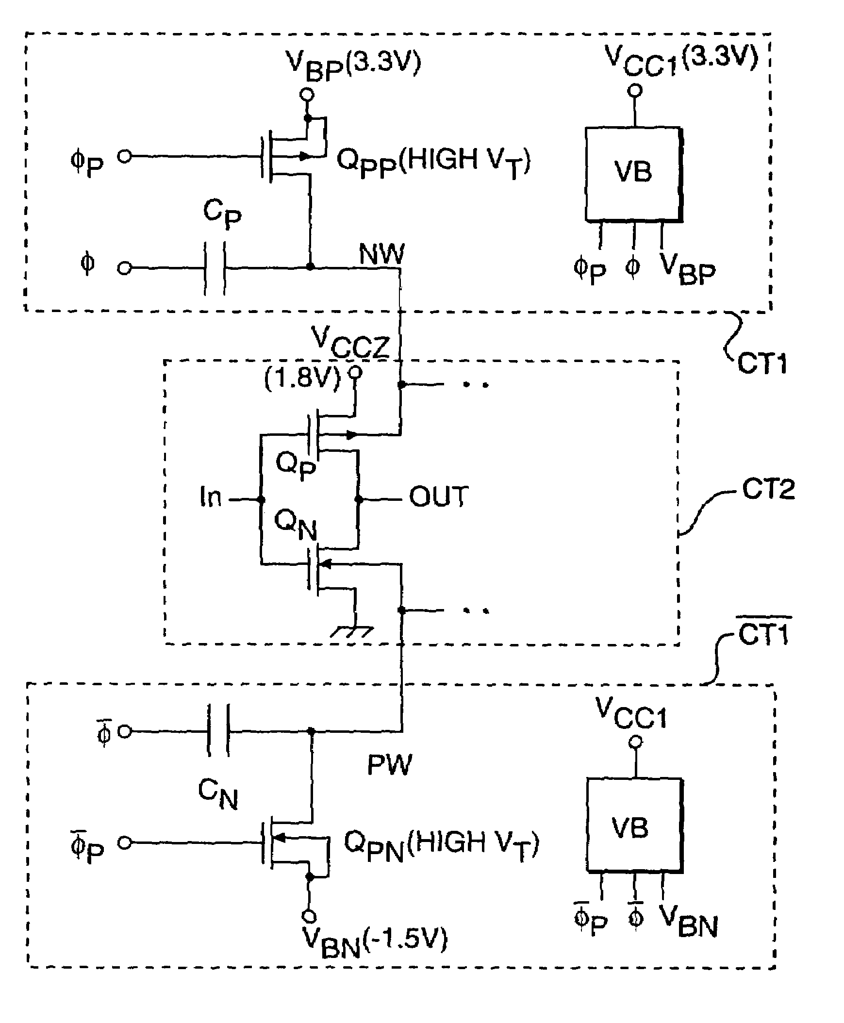
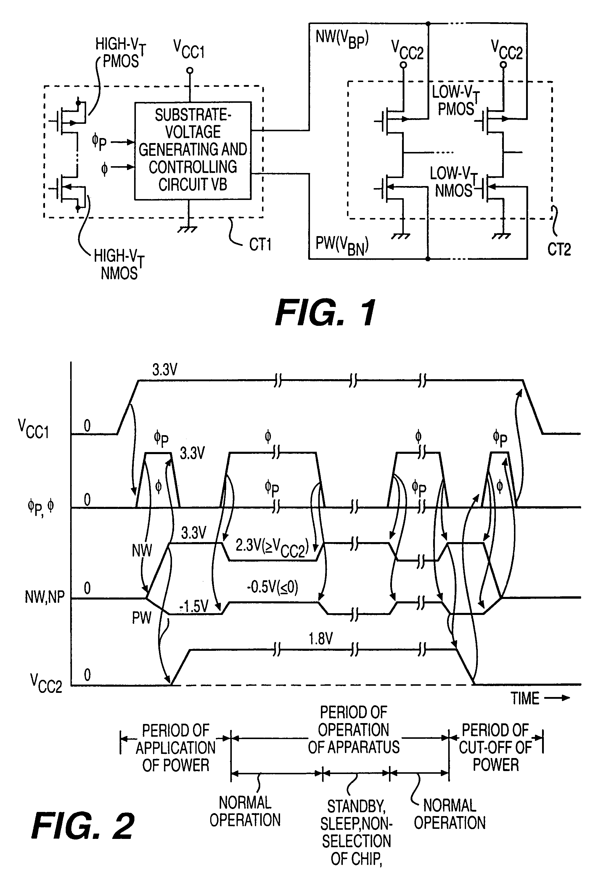
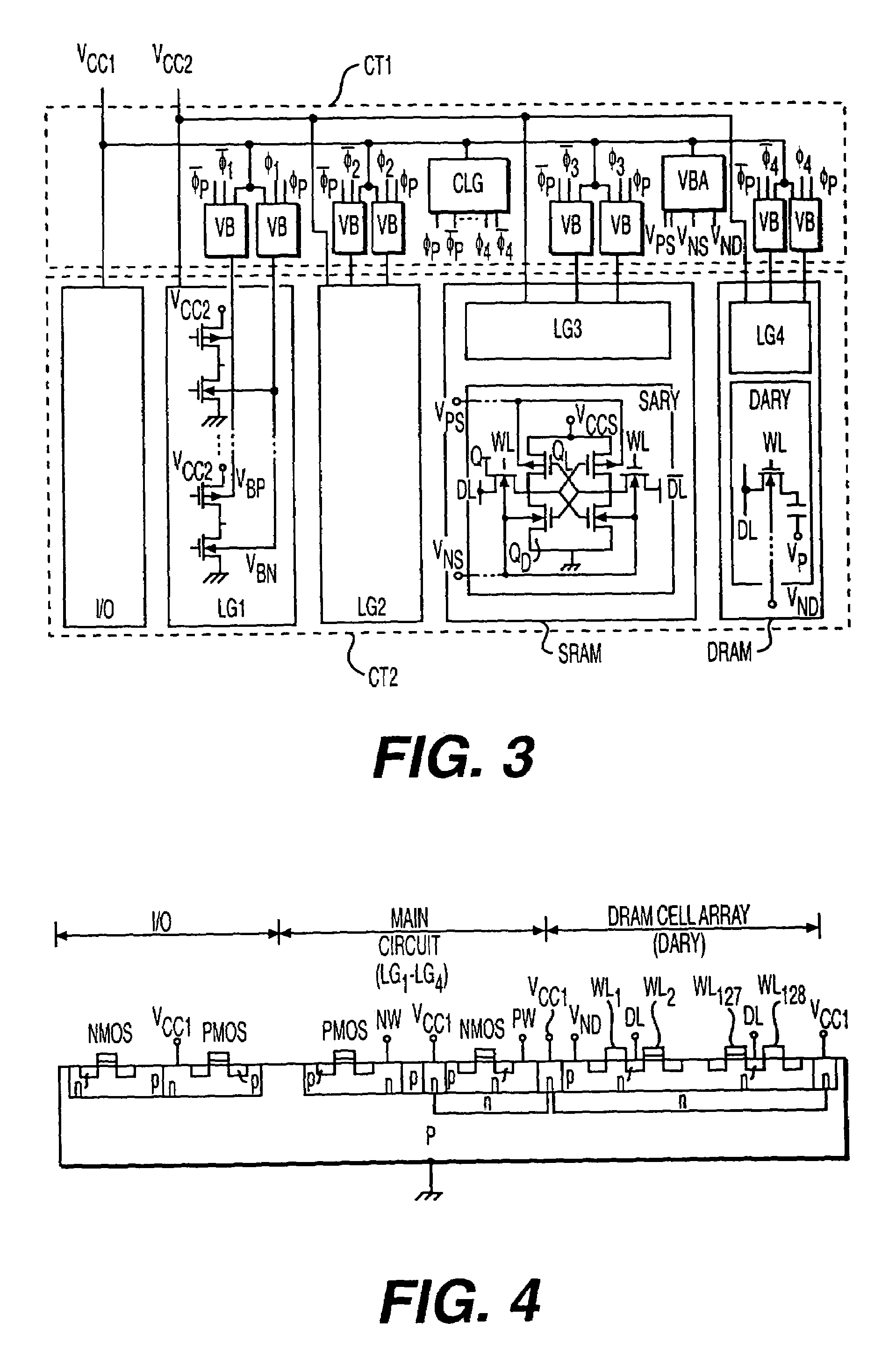
[0062]In the preferred embodiment illustrated in FIG. 1, a circuit block CT1 operating with a high supply voltage VCC1 (e.g., 3.3 V) employs MOSFETs each having a selectable threshold voltage VT as high as 0.5 V, for example, during operation. Since the supply (operating) voltage is sufficiently high, high-speed operation is possible without dropping the threshold voltage to 0.1 V or thereabouts. Therefore, any subthreshold current that exists is sufficiently small to be ignored, without especially switching the threshold voltage during normal operation to the standby voltage, whereby the source of the transistor and its substrate can be connected at a common voltage.

[0063]FIG. 1 also shows a substrate voltage generating and control circuit VB, which is operated with control signals φP, φ.

[0064]A circuit block CT2 operating with a low supply voltage VCC2 (e.g., 1.8 V), on the other hand, has internal transistors that are operated at high speed by dropping their threshold voltage to,...


PUM


Abstract

The well voltage of a CMOS circuit having low-threshold-voltage MOSFETs is controlled when the power supply is turned on, during normal operation, and when the supply voltage is cut off. The CMOS circuit can thus operate stably with lower power consumption, because latching-up is reduced when the supply voltage is applied to the CMOS circuit or when the supply voltage is cut off, and subthreshold current is decreased during normal operation.

Description

[0001]This is a continuation application of U.S. Ser. No. 10 / 385,493, filed Mar. 12, 2003 now abandoned; which is a continuation application of U.S. Ser. No. 09 / 495,957, filed Feb. 2, 2000, now U.S. Pat. No. 6,545,525; which is a continuation of U.S. Ser. No. 09 / 027,212, filed Feb. 20, 1998, now U.S. Pat. No. 6,046,627.BACKGROUND OF THE INVENTION[0002]1. Field of the Invention[0003]The present invention relates generally to semiconductor devices, and, more particularly, to semiconductor devices that combine high-speed performance and low power consumption.[0004]2. Description of the Related Art[0005]An example of reducing power consumption by substrate bias control is described in 1996 IEEE International Solid-State Circuit, Digest of Technical Papers, (1996), pp. 166–167.[0006]With the recent popularity of low-power CMOS LSIs (Complementary Metal Oxide Semiconductor Large Scale Integrated circuits), a trend has developed to maintain high-speed operation by decreasing the threshold ...

Claims


Application Information

Patent Timeline
IPC IPC(8): H03K3/01G05F3/20G11C5/14G11C11/407G11C11/408H01L21/8238H01L27/092H02M3/07H03K17/08H03K17/22H03K19/00H03K19/003H03K19/0948
CPCG11C5/146G11C5/147H03K19/00315H03K19/0013H03K19/0016H01L27/092G05F3/205H02M3/073H01L21/8232
Inventor ITOH, KIYOOMIZUNO, HIROYUKI
Owner RENESAS ELECTRONICS CORP
Why Eureka
Try Eureka