LCD with relay layer connecting pixel electrode with storage capacitor that also covers the storage capacitor

a technology of relay layer and storage capacitor, applied in the field of electro-optical devices, can solve the problems of light leakage current, one of the obstacles to high-quality image display and high-frequency driving, and many technical problems that have to be solved, so as to reduce the influence of transverse electric field, increase the longitudinal electric field generated, and reduce the volume of electro-optical materials

Active Publication Date: 2007-02-13
SEIKO EPSON CORP
View PDF13 Cites 20 Cited by
  • Summary
  • Abstract
  • Description
  • Claims
  • Application Information

AI Technical Summary

Benefits of technology

[0011]First, the electro-optical device of an aspect of the present invention can be driven in an active matrix by including the scanning lines, the data lines, the pixel electrodes, and the thin film transistors. Furthermore, in the above electro-optical device, it is possible to achieve miniaturization of the whole apparatus by including the aforementioned various constituents as part of the laminated structure. It is also possible to enhance the pixel aperture ratio by arranging the various constituent appropriately.
[0109]As a result, it is possible to surely reduce the operational failure due to the transverse electric field in the electro-optical materials, such as liquid crystal by the formation of the convex portion, and also, it is possible to suppress the occurrence of the operational failure due to the step differences in the electro-optical materials, such as liquid crystal by the gentle step differences, so that it is possible to implement electro-optical device, such as liquid crystal apparatus capable of displaying images with high contrast, high brightness, and high quality.

Problems solved by technology

In order to meet the demands, many technical problems have to be solved.
Specifically, for example, there is a problem of the so-called light leakage current which is generated when light enters the semiconductor layers constituting the aforementioned TFTs.
The light leakage current is one of the obstacles to the high quality image display and the high frequency driving.
However, the implementation is difficult because of the complexity in the laminated structure and the problems associated with the aperture ratio as described above.

Method used


Image

  • LCD with relay layer connecting pixel electrode with storage capacitor that also covers the storage capacitor
  • LCD with relay layer connecting pixel electrode with storage capacitor that also covers the storage capacitor
  • LCD with relay layer connecting pixel electrode with storage capacitor that also covers the storage capacitor

Examples


Embodiment Construction

[0143]Now, the exemplary embodiments of the present invention will be described with reference to the figures. The following exemplary embodiment is an electro-optical device according to an aspect of the present invention which is applied to a liquid crystal apparatus.

Constitution of Pixel Portion

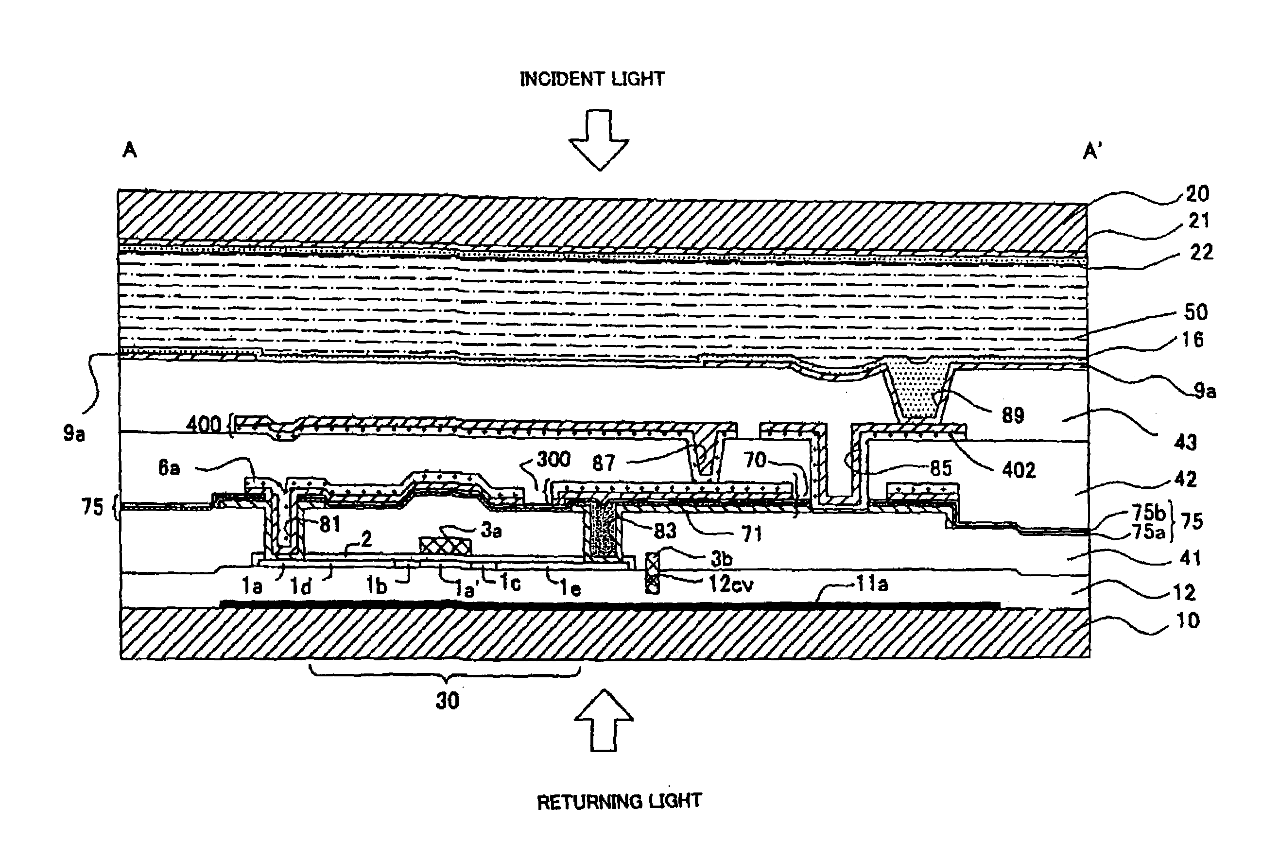
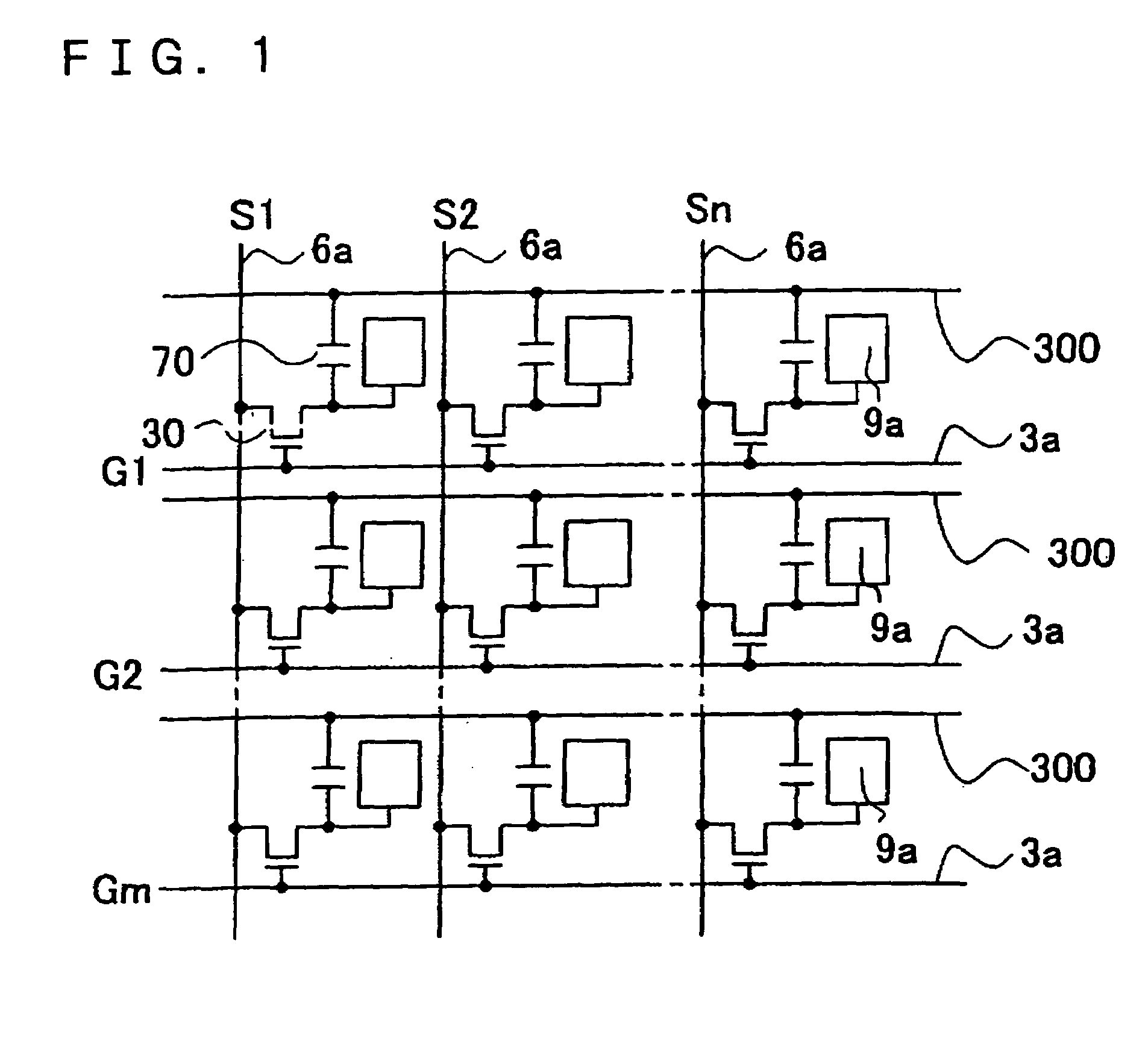
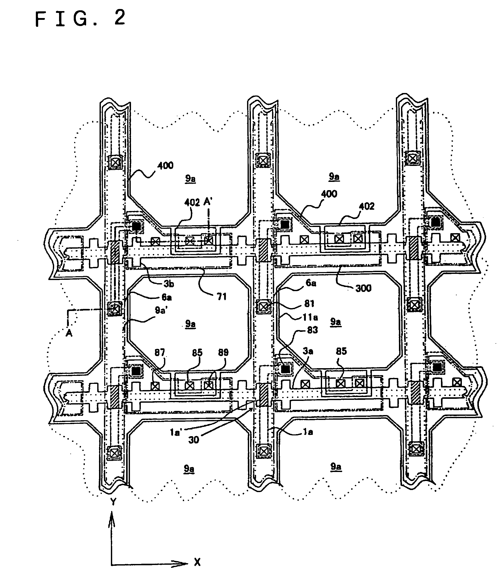
[0144]First, the constitution of the electro-optical device in an exemplary embodiment of the present invention will be described with reference to FIGS. 1 to 4. Herein, FIG. 1 is a circuit schematic illustrating an equivalent circuit of various elements and wiring lines which are provided in a plurality of pixels arranged in a matrix which constitute image display regions in the electro-optical device. FIG. 2 is a plan view illustrating a plurality of pixel groups which are adjacent to each other on a TFT array substrate on which data lines, scanning lines, pixel electrodes, etc., are formed in the electro-optical device. FIG. 3 is a plan view illustrating the only principal parts extract...


PUM

PropertyMeasurementUnit
thicknessaaaaaaaaaa
thicknessaaaaaaaaaa
dielectric constantaaaaaaaaaa

Abstract

An electro-optical device including, above a substrate: data lines extending in a first direction, scanning lines extending in a second direction which intersects the data lines, pixel electrodes and thin film transistors provided so as to correspond to intersection regions of the data lines and the scanning lines, and storage capacitors electrically connected to the thin film transistors and the pixel electrodes. Dielectric films which constitute the storage capacitors are made of a plurality of layers including different materials and one of the plurality of the layers is made of a material having a higher dielectric constant than those of the other layers.

Description

BACKGROUND OF THE INVENTION[0001]1. Field of Invention[0002]The present invention relates to a technical field of electro-optical devices such as liquid crystal devices, and electronic apparatuses. The present invention also relates to a technical field of an electrophoresis device, such as an electronic paper, an EL (electroluminescent) device, and a device using an electron emission element (a field emission display and a surface-conduction electron-emitter display).[0003]2. Description of Related Art[0004]In the related art, an electro-optical device, such as a liquid crystal device capable of displaying an image, in which an electro-optical material, such as liquid crystal, is interposed between a pair of substrates and light is transmitted so as to pass through the substrates and the electro-optical material, is disclosed. “Displaying the image” is realized, for example, by changing the state of an electro-optical material in each pixel to change the transmittance ratio of ligh...

Claims


Application Information

Patent Timeline
Patent Type & Authority Patents(United States)
IPC IPC(8): G02F1/1343G02F1/1368G02F1/133G02F1/1362H01L21/336H01L29/786
CPCG02F1/136213G02F1/136209G02F1/136227G02F1/133
Inventor TAKAHARA, KENICHIKURASHINA, HISAKISHIMIZU, YUICHI
Owner SEIKO EPSON CORP
Why Eureka
Try Eureka