Integrated circuit with improved interconnect structure and process for making same

a technology of integrated circuits and interconnects, applied in the direction of semiconductor devices, semiconductor/solid-state device details, electrical devices, etc., can solve the problems of limiting the size of the area that can become small using conventional processes, high processing costs, poor yield, etc., to reduce cycle time, reduce wafer cycle time, cost-effective

Inactive Publication Date: 2007-02-20
UNITED MICROELECTRONICS CORP
View PDF40 Cites 26 Cited by
  • Summary
  • Abstract
  • Description
  • Claims
  • Application Information

AI Technical Summary

Benefits of technology

[0019]Another object of the present invention is to provide an interconnect/packaging structure and method that is simple, cost-effective, fast, and that does not require the critical resources of a conventional semiconductor fab to perform;
[0020]A related object is to provide an interconnect and packaging method that can be can be completed before normal wafer processing operations were undertaken to reduce wafer

Problems solved by technology

This approach, however, suffers from extremely high processing costs, and very poor yield.
However, there is a limit to how small this area can become using conventional processes, because the pads have to be large enough to accommodate a wire bond, or a flip chip type solder bump.
Thus, there is inevitably a large amount of surface area, otherwise usable for forming electronic circuits, that is wasted in a chip scale type package as shown in FIG. 1.
The vias, appear to be limited to connecting any circuits to a groundplane, however (as evidenced by the single metallization layer shown at the backside of the substrate) and not for connecting such circuits to another circuit (or set of circuits).
It is apparent that this approach, too, is commercially impractical for conventional processing because the fabricating steps are complicated.
None of the above references, nonetheless, appear to address the problem of how to optimize the usable chip surface area, or how to minimize interconnect areas required to contact other chips.
While certain patents issued to Tessera, Inc. are directed generally to this problem (see e.g., U.S. Pat. Nos. 5,148,265; 5,148,266; 5,

Method used


Image

  • Integrated circuit with improved interconnect structure and process for making same
  • Integrated circuit with improved interconnect structure and process for making same
  • Integrated circuit with improved interconnect structure and process for making same

Examples


Embodiment Construction

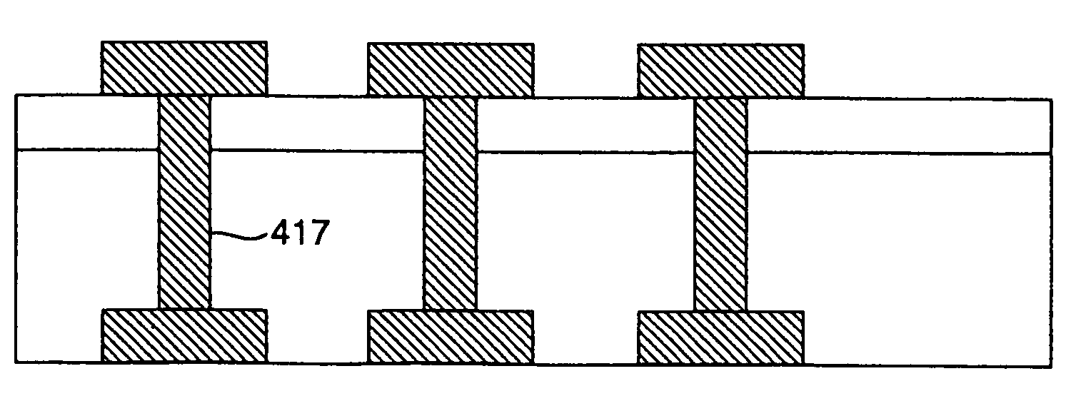
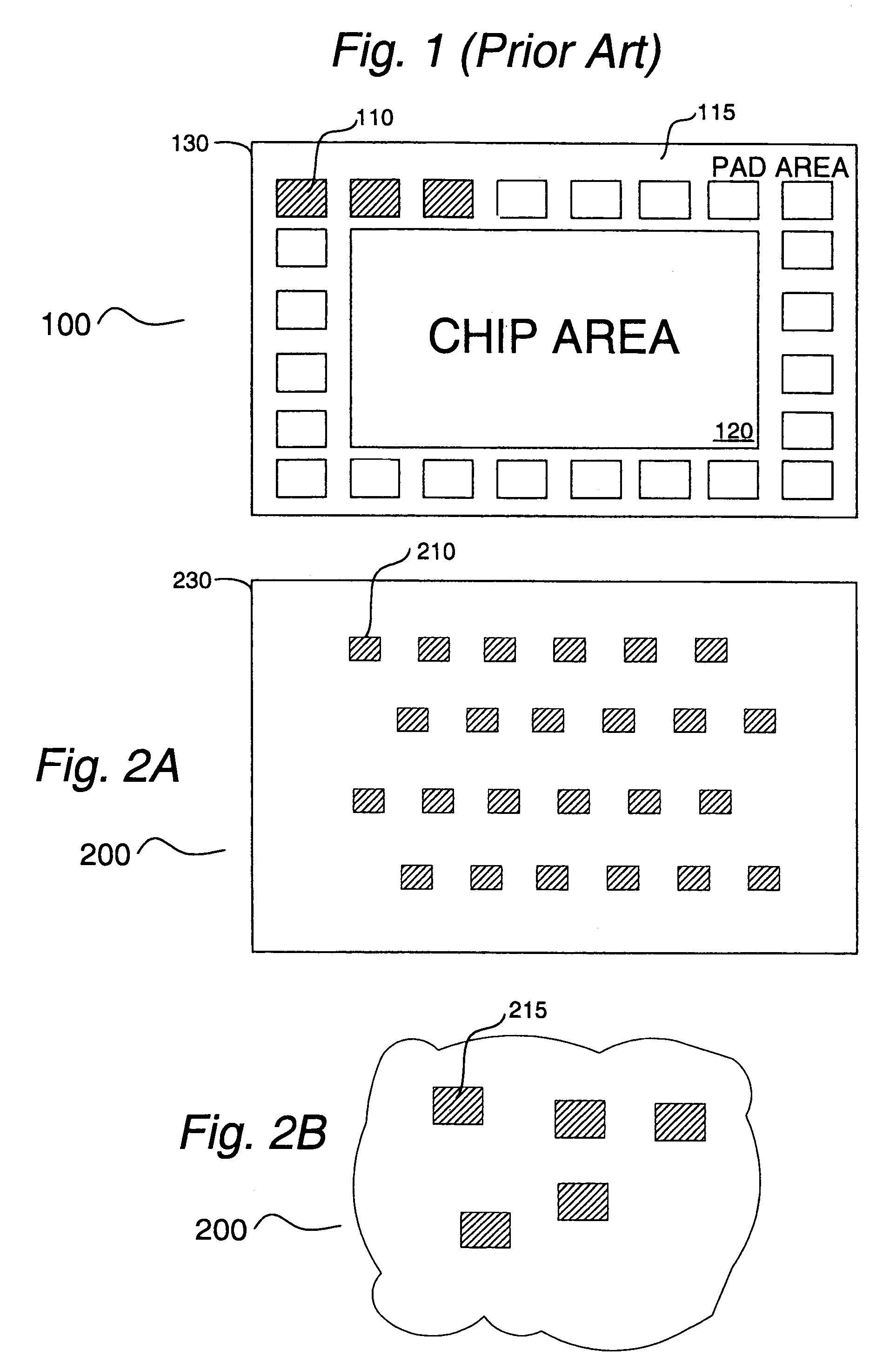
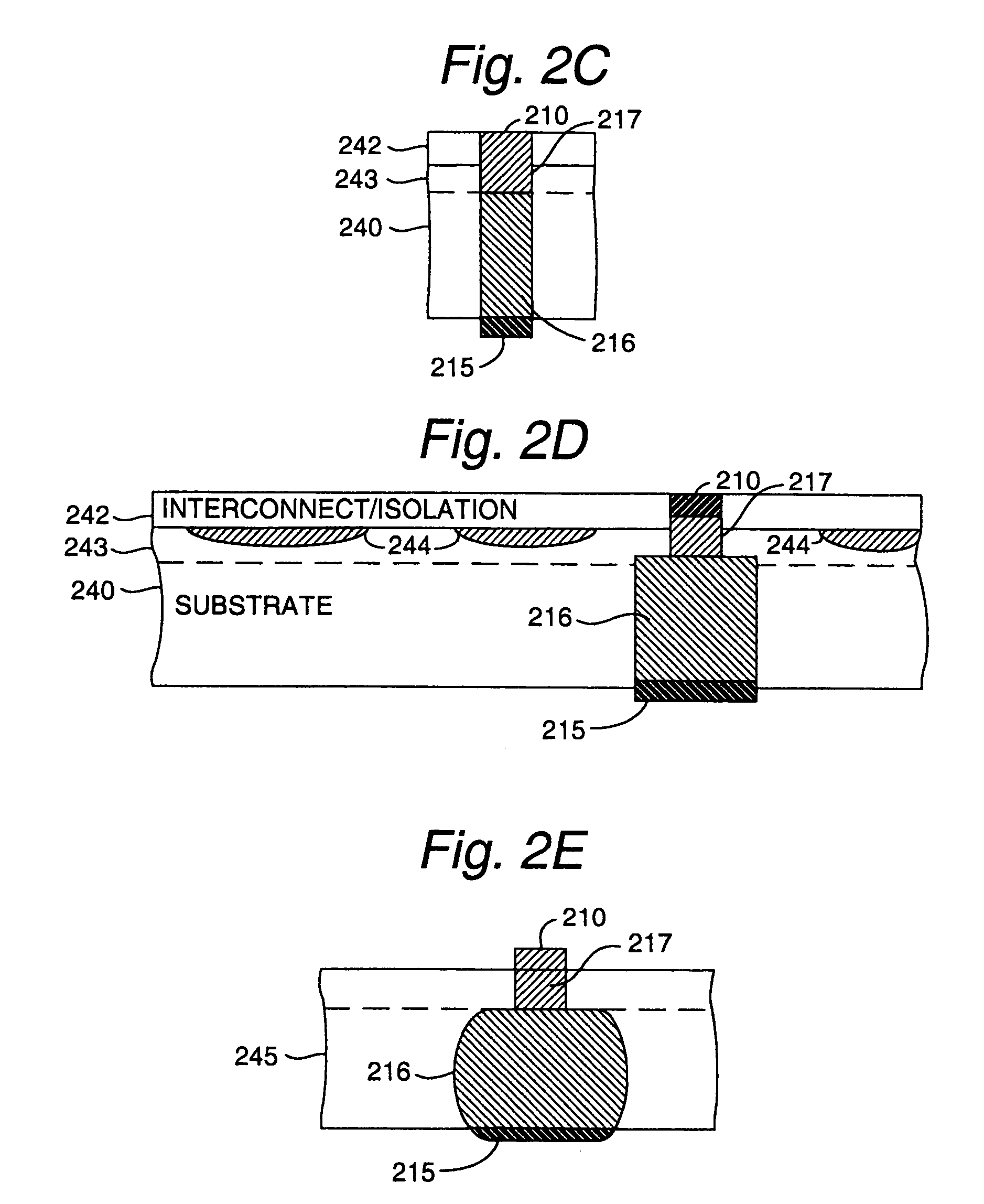
[0032]A top view of an integrated circuit (IC) 200 formed in accordance with the present invention is depicted generally in FIG. 2A. Such circuit 200 includes a die 230, which is formed along with a plurality of other die (not shown) using conventional masking, deposition and etching operations performed on a silicon wafer during a semiconductor manufacturing process. For ease of reference and comparison with prior art IC 100, a series of top surface interconnect nodes 210 are depicted as well. Such top surface interconnect nodes 210 are located on a top surface of die 230, and are distributed according to desired signal connections with electronic circuits formed in (and on) die 230. Top surface interconnect nodes 210 are formed from such conventional conductive materials such as aluminum, gold, or some other suitable low resistance material.

[0033]In a preferred embodiment, top surface interconnect nodes 210 are preferably much smaller than comparable I / O bonding pads of prior art ...


PUM


Abstract

A semiconductor die and an associated low resistance interconnect located primarily on the bottom surface of such die is disclosed. This arrangement provides a flexible packaging structure permitting easy interconnected with other integrated circuits; in this manner, a number of such circuits can be stacked to create high circuit density multi-chip modules. A process for making the device is further disclosed. To preserve structural integrity of a wafer containing such die during manufacturing, a through-hole via formed as part of the interconnect is filled with an inert material during operations associated with subsequent active device formation on such die.

Description

RELATED APPLICATION DATA[0001]The present application is a continuation of Ser. No. 10 / 166,973 filed Jun. 11, 2002, now U.S. Pat. No. 6,838,310, which application in turn is a divisional of Ser. No. 09 / 304,244 filed May 3, 1999 now U.S. Pat. No. 6,429,509, both of which are incorporated by reference herein.FIELD OF THE INVENTION[0002]The invention relates generally to the area of semiconductor device interconnects and packaging techniques. More particularly, the invention discloses an integrated circuit die that is formed with controllable sized and spaced through-holes extending through a substrate of such die, so that such die can be easily and optimally interconnected and packaged.BACKGROUND OF THE INVENTION[0003]Contemporary integrated circuits (ICs) include collections of interconnected electronic circuits embodied in semiconductor structures formed during processing of a silicon substrate wafer. The formation of a particular IC can require several hundred discrete complex proc...

Claims


Application Information

Patent Timeline
IPC IPC(8): H01L21/302H01L21/461
CPCH01L23/481H01L24/10H01L24/13H01L25/0657H01L2224/13099H01L2225/06513H01L2225/06541H01L2924/01013H01L2924/01022H01L2924/01029H01L2924/01074H01L2924/01078H01L2924/01079H01L2924/01082H01L2924/14H01L2924/30105H01L2924/30107H01L2924/01005H01L2924/01006H01L2924/01033H01L2924/014H01L2924/00H01L2224/13
Inventor HSUAN, MIN-CHIH JOHN
Owner UNITED MICROELECTRONICS CORP
Why Eureka
Try Eureka