Timing variation measurement system and method

a timing variation and measurement system technology, applied in the field of semiconductor devices, can solve the problems of various signal timing variations, adversely affecting the timing of various operations, and fabrication process discrepancies that produce timing delay variations, and achieve accurate modeling of chip variations, the effect of facilitating the measurement of timing variations

Inactive Publication Date: 2007-02-27
CISCO TECH INC
View PDF13 Cites 28 Cited by
  • Summary
  • Abstract
  • Description
  • Claims
  • Application Information

AI Technical Summary

Benefits of technology

[0009]The present invention is a system and method that facilitates measurement of timing variations (e.g., timing delays) in a semiconductor chip. The present invention can be utilized to monitor timing variations spatially between different locations inside a chip. The present invention provides insight into timing variations inside a semiconductor chip and across different chips. Timing degradation and variations that affect reliability can also be captured over longer periods of time, during end use in the field after manufacturing. In addition, the timing variation information can be utilized to accurately model on chip variations in subsequently manufactured semiconductor chips and assist with timing closure procedures. For example, the timing variation information can be utilized to compare various semiconductor processes with respect to process variation ranges.

Problems solved by technology

However, a number of conditions can adversely impact the timing of various operations.
For example, fabrication process deviations, voltage drops, and temperature can cause various signal timing variations (e.g., delays) in semiconductor components.
For example, changes in device parameters (e.g., transistor parameters) and interconnect metal layer characteristics (e.g., dielectric characteristics) often result in fabrication process discrepancies that produce timing delay variations.
The fabrication process discrepancies often produce timing differences or shifts across wafer to wafer, chip to chip, and / or within a chip.
Timing variations or differences can have detrimental impacts on the performance of the semiconductor components and uniformity of results.
It is traditionally very difficult for a designer to determine if problems in a silicon chip performance are related to uneven timing delays.
Traditional attempts at measuring timing delays are usually limited and require significant internal and external chip resources.
For example, conventional wafer test measurements are often limited to a relatively few places or locations on a wafer (e.g., a process corner).
This does not typically provide very good insight to process variations that are encountered in other areas of a chip and from chip to chip.
In addition, the actual layout of chip components (e.g., logic units, functional components, gates, etc) can vary (e.g., between chips manufactured at different foundries) making it more difficult to determine impacts on any particular component related to timing variations since the location of a component with respect to a corner measurement can vary.
However, the logistics of traditional attempts at directly measuring and retrieving analog frequency information from ring oscillators makes it very difficult and expensive.
Also, the measurements are typically performed as wafer tests and not performed across wafer lots, making it very difficult for a designer to identify and analyze delay variations for a component across different wafer lots.
In addition, information typically available to designers is usually very limited due to the I / O resource consumption requirements of traditional approaches.
For example, delay test bumps are not coupled to package pins and so even through a ring oscillator is present in a die, timing variation measurements are not available once the die is packaged.
However, timing variations can change over time and adversely impact use of a product in the field after manufacturing.
At the same time, decreases in component sizes are making components more sensitive to process, voltage and temperature variations that result in even greater timing delay impacts.

Method used


Image

  • Timing variation measurement system and method
  • Timing variation measurement system and method
  • Timing variation measurement system and method

Examples


Embodiment Construction

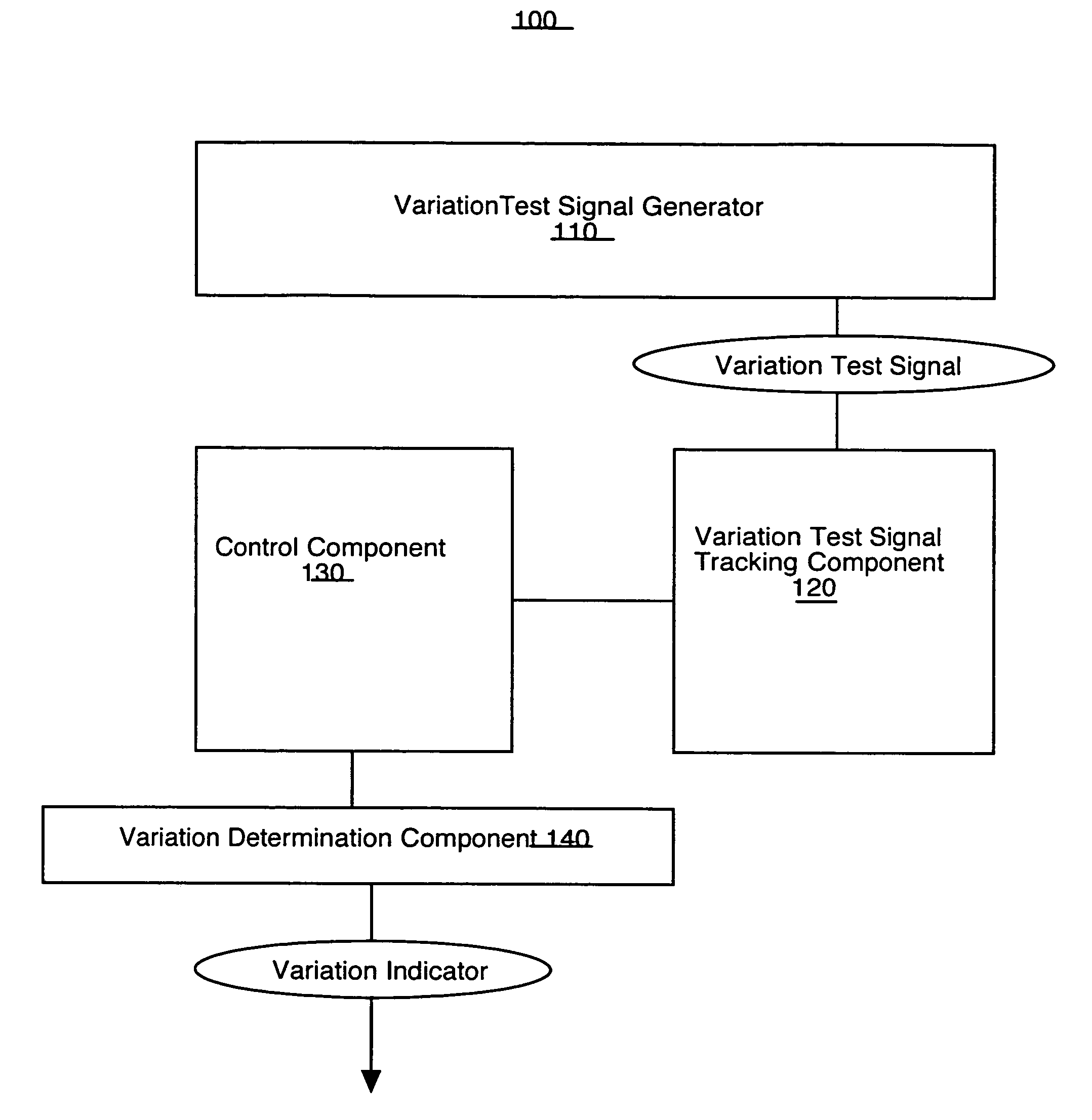
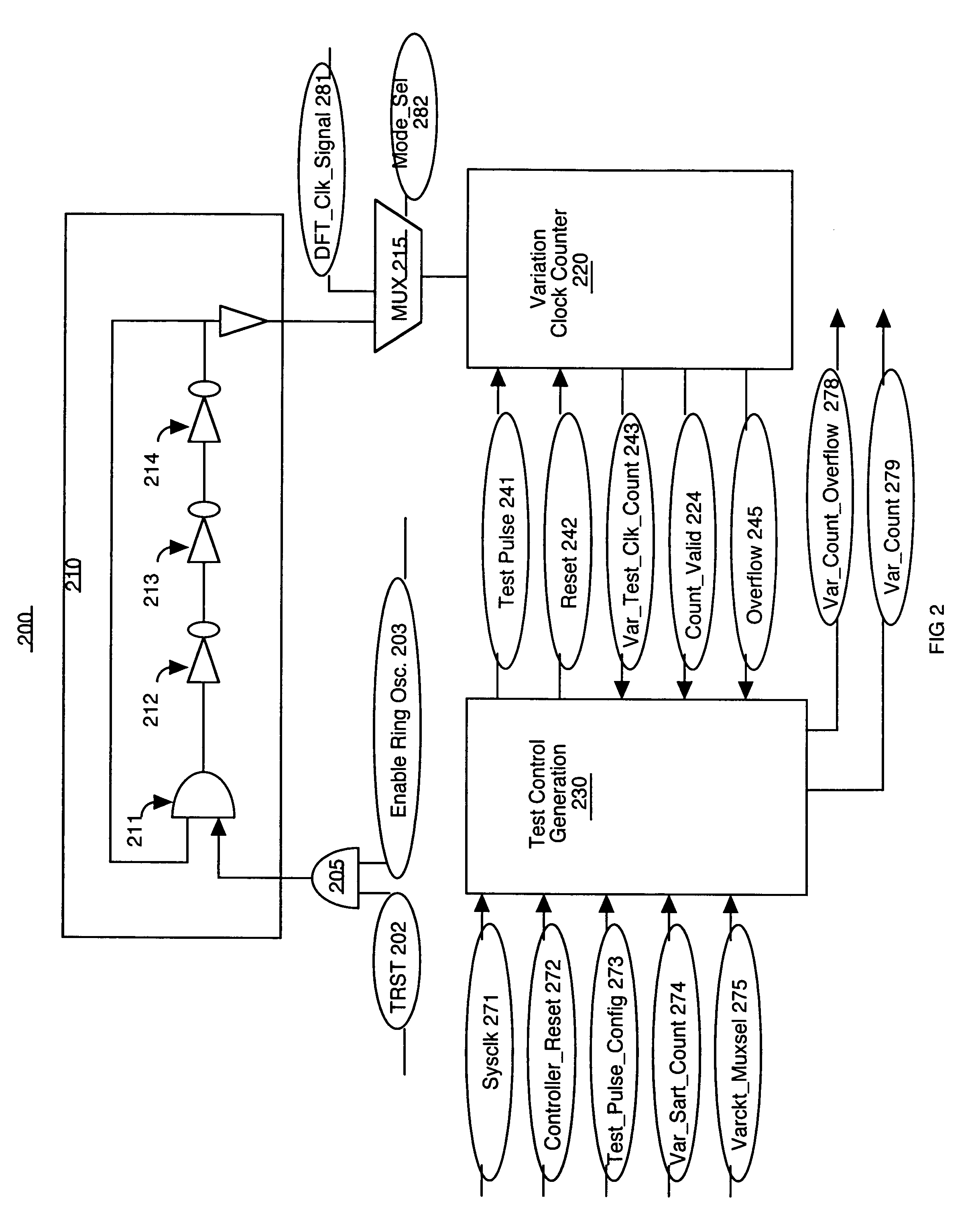
[0016]Reference will now be made in detail to the preferred embodiments of the invention, examples of which are illustrated in the accompanying drawings. While the invention will be described in conjunction with the preferred embodiments, it will be understood that they are not intended to limit the invention to these embodiments. On the contrary, the invention is intended to cover alternatives, modifications and equivalents, which may be included within the spirit and scope of the invention as defined by the appended claims. Furthermore, in the following detailed description of the present invention, numerous specific details are set forth in order to provide a thorough understanding of the present invention. However, it will be obvious to one ordinarily skilled in the art that the present invention may be practiced without these specific details. In other instances, well known methods, procedures, components, and circuits have not been described in detail as not to unnecessarily o...


PUM


Abstract

The present invention is a system and method that facilitates measurement of timing variations (e.g., timing delays) in a semiconductor chip. The timing variations are measured and presented as digital values without extensive off chip measurement and analysis equipment. The timing variation measurements provides insight into timing variations (e.g., delays) inside a semiconductor chip and across different chips, including timing impacts experienced in end use after manufacturing. A timing variation measurement system includes a variation test signal generator for passing a signal through a portion of a circuit and generating a variation test signal. A variation test signal tracking component digitally counts cycles in a variation test signal and a control component controls the counting (e.g., the length of time the cycles are counted). Timing variation information, including a digital value associated with the variation test signal cycle count, can be communicated via pins and / or a processor interface.

Description

FIELD OF THE INVENTION[0001]This invention relates to the field of semiconductor devices. In particular, the present invention relates to measuring timing variations in a semiconductor chip.BACKGROUND OF THE INVENTION[0002]Electronic systems and circuits have made a significant contribution towards the advancement of modern society and are utilized in a number of applications to achieve advantageous results. Numerous electronic technologies such as digital computers, calculators, audio devices, video equipment, and telephone systems facilitate increased productivity and cost reductions in analyzing and communicating data, ideas and trends in most areas of business, science, education and entertainment. The timing of operations within a system or circuit is often critical to the proper performance of a device in providing proper results. However, a number of conditions can adversely impact the timing of various operations. For example, fabrication process deviations, voltage drops, a...

Claims


Application Information

Patent Timeline
Patent Type & Authority Patents(United States)
IPC IPC(8): G01R23/175
CPCG01R31/31725
Inventor BHANDARI, AJAY
Owner CISCO TECH INC
Why Eureka
Try Eureka