Nitride semiconductor device and method of manufacturing the same

a technology of nitride semiconductor and semiconductor, which is applied in the direction of semiconductor/solid-state device manufacturing, semiconductor devices, electrical devices, etc., can solve the problems of reducing the inner quantum efficiency, affecting the refractive index of the nitride semiconductor, and serious limitations in the inner quantum efficiency

Inactive Publication Date: 2007-03-06
SAMSUNG ELECTRONICS CO LTD
View PDF11 Cites 37 Cited by
  • Summary
  • Abstract
  • Description
  • Claims
  • Application Information

AI Technical Summary

Benefits of technology

[0013]Therefore, the present invention has been made in view of the above problems, and it is an object of the present invention to provide a nitride semiconductor device having a micro-structured current diffusion pattern formed in a clad layer, thereby accomplishing uniform current diffusion.
[0014]It is another object of the present invention to provide a method of manufacturing a nitride semiconductor device that is capable of forming a micro-structured insulation pattern in a clad layer to improve current diffusion efficiency and repetitively forming the insulation pattern on the surface of an upper clad layer to increase surface roughness, thereby improving light extraction efficiency.
[0016]Preferably, the current diffusion pattern is composed of a silicon nitride (SiNx) arranged in a nano-sized dot structure. The silicon nitride pattern is formed on the surface of the second p-type nitride semiconductor layer, and the surface of the second p-type nitride semiconductor layer is etched using the silicon nitride pattern as a mask such that a light emitting surface has predetermined surface roughness, whereby light extraction efficiency is improved.

Problems solved by technology

The inner quantum efficiency is seriously limited due to ununiform current diffusion.
Consequently, the entirety of the active layer does not serve as a light-emitting region, which decreases the inner quantum efficiency.
However, the refractive index of the nitride semiconductor has a limited changeable range.
However, it is necessary to perform pattern formation through the use of Metal Organic Chemical Vapor Deposition (MOCVD) or other CVD processes in order to increase the surface roughness, which is very troublesome.

Method used


Image

  • Nitride semiconductor device and method of manufacturing the same
  • Nitride semiconductor device and method of manufacturing the same
  • Nitride semiconductor device and method of manufacturing the same

Examples


example

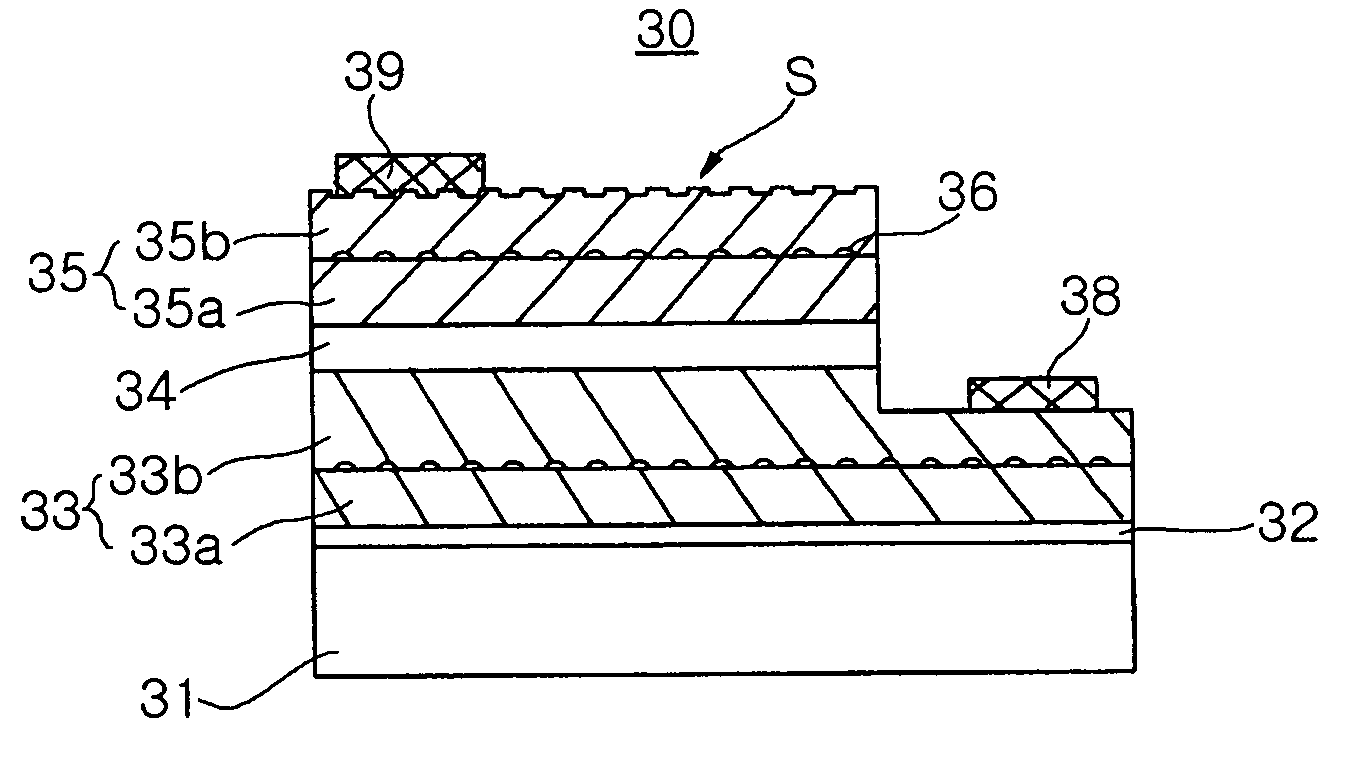
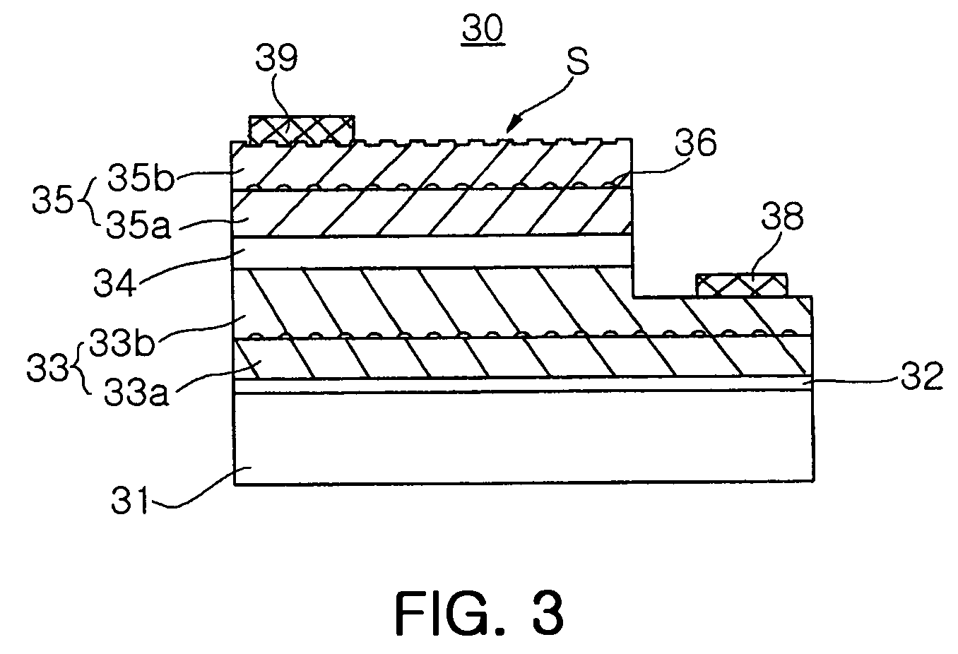
[0049]Two nitride semiconductor devices were manufactured under the same conditions to confirm the effect of the current diffusion pattern according to the present invention.

[0050]A sapphire substrate was placed in a Metal Organic Chemical Vapor Deposition (MOCVD) chamber, and trimethylaluminum and ammonia gas were supplied to form a buffer layer having a thickness of approximately 20 nm at a temperature of 550° C. After that, an epitaxial layer for the nitride semiconductor layer was grown. Specifically, trimethyl gas and ammonia gas were supplied to form an n-type GaN layer having a thickness of 1.5 μm at a temperature of approximately 1100° C. At this time, Si was used as an n-type impurity. Subsequently, the injection amount of trimethylindium was adjusted to form a multi-quantum well structure consisting of InGaN / GaN.

[0051]Next, a nitride semiconductor device identical to the conventional nitride semiconductor device (hereinafter, referred to as “comparative example”) and a nit...


PUM

PropertyMeasurementUnit
thicknessaaaaaaaaaa
thicknessaaaaaaaaaa
thicknessaaaaaaaaaa

Abstract

The present invention provides a nitride semiconductor device. The nitride semiconductor device comprises an n-type nitride semiconductor layer formed on a nitride crystal growth substrate. An active layer is formed on the n-type nitride semiconductor layer. A first p-type nitride semiconductor layer is formed on the active layer. A micro-structured current diffusion pattern is formed on the first p-type nitride semiconductor layer. The current diffusion pattern is made of an insulation material. A second p-type nitride semiconductor layer is formed on the first p-type nitride semiconductor layer having the current diffusion pattern formed thereon.

Description

RELATED APPLICATION[0001]The present application is based on, and claims priority from, Korean Application No. 2004-53392, filed on Jul. 9, 2004, the disclosure of which is incorporated by reference herein in its entirety.BACKGROUND OF THE INVENTION[0002]1. Field of the Invention[0003]The present invention relates to a nitride semiconductor device, and more particularly to a nitride semiconductor device having improved current diffusion and increased surface roughness, whereby electric and optical characteristics are improved. Also, the present invention relates to a method of manufacturing the same.[0004]2. Description of the Related Art[0005]Generally, a nitride semiconductor is widely used as a material for manufacturing visible-light, ultraviolet-light, and cyan optical devices, such as a light emitting diode (LED) or a laser diode (LD), since the nitride semiconductor has the characteristics of emitting light having a wide range from visible light to ultraviolet light. The nitr...

Claims


Application Information

Patent Timeline
Patent Type & Authority Patents(United States)
IPC IPC(8): H01L33/00H01L33/06H01L33/32
CPCH01L33/14H01L33/32H01L33/20Y10S438/962Y10S438/964
Inventor KIM, JE WONKIM, SUN WOONKIM, DONG JOON
Owner SAMSUNG ELECTRONICS CO LTD
Why Eureka
Try Eureka