Floating gate transistors

a technology of floating gate transistor and gate gate, which is applied in the field of floating gate transistor, can solve the problems of not really being taken off, affecting the threshold voltage of the transistor, and difficult programming and control of the charge on the floating gate, so as to achieve the effect of enhancing leakage through the insulating layer

Inactive Publication Date: 2007-03-20
TOUMAZ TECH
View PDF9 Cites 47 Cited by
  • Summary
  • Abstract
  • Description
  • Claims
  • Application Information

AI Technical Summary

Benefits of technology

[0040]The insulating region will permit charge leakage from the floating gate to a very small extent. However, providing that this leakage is sufficient, the floating gate will charge to the operating voltage. The leakage through the insulating layer can be enhanced to a s

Problems solved by technology

However such a stacked floating gate structure is not recommended, as the process steps required to fabricate the top gate can cause changes in the floating gate and substrate which affect the transistor's threshold voltage.
Despite the obvious attractions, the usage of floating gate structures in analogue circuits has not really taken off, due to a number of practical problems in the implementation of analogue floating gate circuits.
In particular, programming and control of the charge on the floating gate is very difficult, and typically involves a combination of Fowler-Nordheim tunnelling and hot carrier injection.
Although this process is similar to the methods used for programming and erasing digital ROMs, repeated programming causes degradation of the silicon oxide leading to transistor breakdown.
This leads to long-term reliability problems for circuits which require constant tuning or alteration.
In addition the ap

Method used


Image

  • Floating gate transistors
  • Floating gate transistors
  • Floating gate transistors

Examples


Embodiment Construction

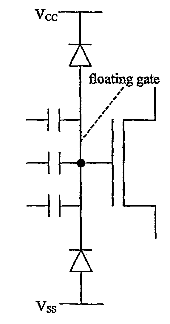
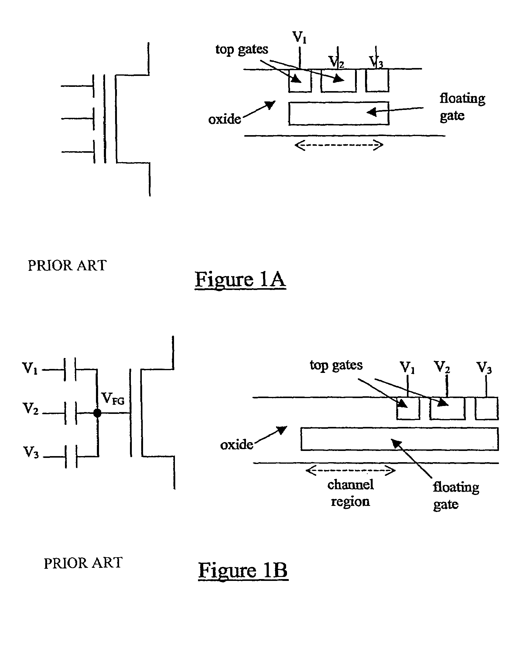
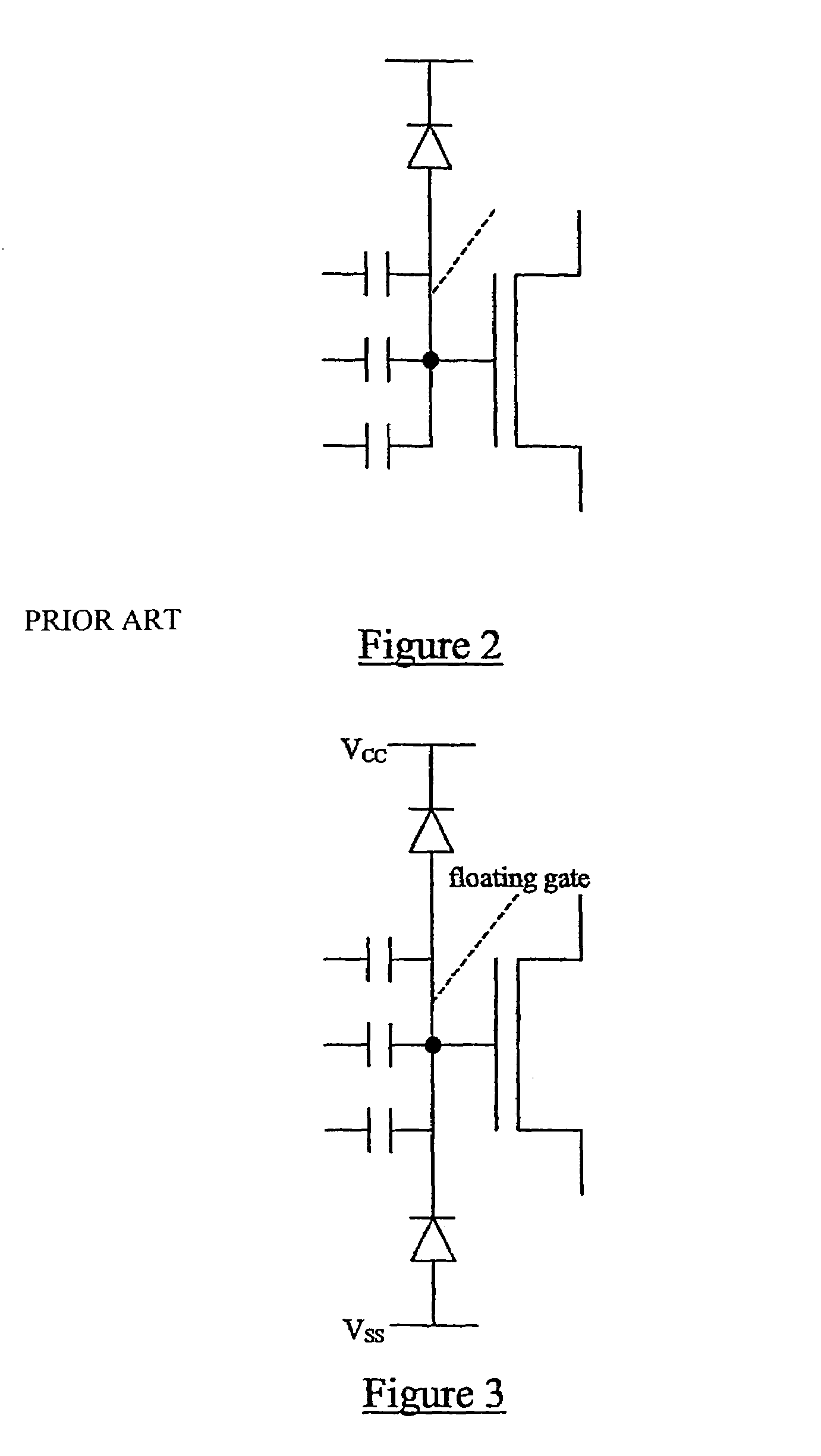
[0054]Prior art floating gate MOS transistors have been described above with reference to FIGS. 1 and 2. Whilst the architecture illustrated in FIG. 2 provides an improvement over that of FIG. 1, that architecture is not ideal because of limitations which it imposes on the voltage(s) which can be applied to the control gate(s).

[0055]An improvement to the architecture of FIG. 2 involves the use of two reverse biased diodes (pn junctions) connected to the floating gate as shown in FIG. 3. These diodes can be connected directly to the power rails VCC, VSS which will thus set an operating point somewhere between the two power supply rails. The diodes operate as non-linear resistances. By manipulating the relative diode dimensions, one of the diodes can be made ‘dominant’, thus defining the power rail which the operating point will approach. Knowing the expected input voltage swing, the divider voltage may be set accordingly. Imposing a voltage perturbation on this structure within the e...


PUM


Abstract

A floating gate MOS transistor comprises one or more control gates, an active channel, and at least one floating gate disposed between the control gate(s) and the active channel. First and second non-linear resistances couple the floating gate to first and second control voltage sources respectively, the non-linear resistances forming a voltage divider network which sets the operating voltage of the floating gate.

Description

BACKGROUND OF THE INVENTION[0001]The present invention relates to floating gate transistors and more particularly to floating gate metal-oxide-semiconductor transistors.[0002]Floating gate metal-oxide-semiconductor (MOS) transistors are devices with a first gate situated on a layer of insulating oxide directly above the transistor channel, and a second control gate situated on a layer of insulating oxide above the first gate. The first gate is electrically isolated, hence the term ‘floating gate’, and any charge deposited on the floating gate will be held almost indefinitely. Floating gate devices are commonly used in digital integrated circuit (IC) design as the storage components of FLASH EPROM. Typically, floating gate MOS transistors are fabricated using thin film technology, with a high degree of integration between transistors and other components.[0003]During the last decade, floating gate devices have also been exploited in analogue IC design to implement circuits and small ...

Claims


Application Information

Patent Timeline
IPC IPC(8): H01L29/76G06G7/60G11C27/00H01L21/28H01L21/336H01L27/115H01L29/423H01L29/788
CPCG06G7/60G11C27/005H01L21/28273H01L29/788H01L29/42324H01L29/66825H01L27/115H01L29/40114H10B69/00
Inventor LANDE, TOR SVERRE
Owner TOUMAZ TECH
Why Eureka
Try Eureka