Dual loop voltage regulation circuit of power supply chip

a voltage regulation circuit and power supply chip technology, applied in pulse generators, pulse techniques, instruments, etc., can solve problems such as output error, output voltage dithering easily, output voltage dithering, etc., to improve dithering, reduce non-overlap time, and output voltage rapid and stable

Inactive Publication Date: 2007-03-20
LEADTREND TECH
View PDF4 Cites 132 Cited by
  • Summary
  • Abstract
  • Description
  • Claims
  • Application Information

AI Technical Summary

Benefits of technology

[0008]In view of the above-mentioned problems, the main object of the present invention is to provide a dual loop voltage regulation circuit of power supply chip. Through the controlling of the switches, the transition of the amplifier is accelerated and the non-overlap time is reduced, and therefore the output voltage is rapid and stable, thus improving the dithering in a conventional stabilizing circuit output voltage and reducing the errors caused by the output.
[0020]With this dual loop voltage regulation circuit of power supply chip and through each loop switch triggered to be on or off by the comparator, the current source loop or the sink loop is provided and the non-overlap time in the voltage regulation circuit and the dithering in the output voltage are reduced, therefore improving the voltage output quality of the voltage regulation circuit.

Problems solved by technology

Due to the use of the single close loop system, there is a need for a relatively large offset voltage to control the output of one of the amplifiers to be high potential, resulting in an overtime of the non-overlap, which makes the output voltage dithering easily.
The non-overlap time will be a long period due to the characteristics of the single close loop, which results in a dithering in the output.
Also the relatively large reference voltage Vref will cause an output error, referring to FIG. 4A showing an oscillogram of the voltage and current of the prior art.
Therefore, the problem about how to provide a voltage regulation circuit with relatively stable output is one of the problems to be solved to researchers.

Method used


Image

  • Dual loop voltage regulation circuit of power supply chip
  • Dual loop voltage regulation circuit of power supply chip
  • Dual loop voltage regulation circuit of power supply chip

Examples


Embodiment Construction

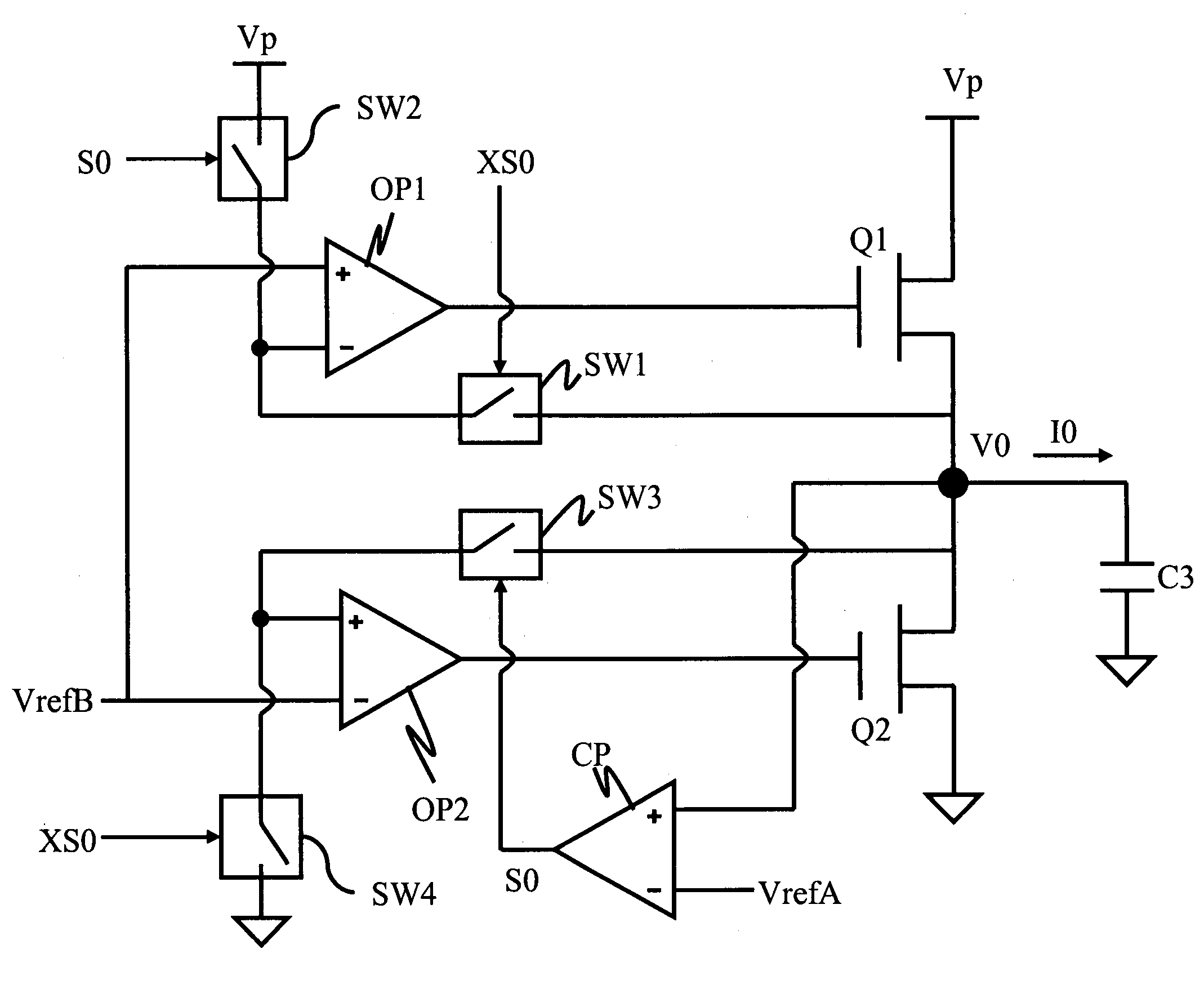
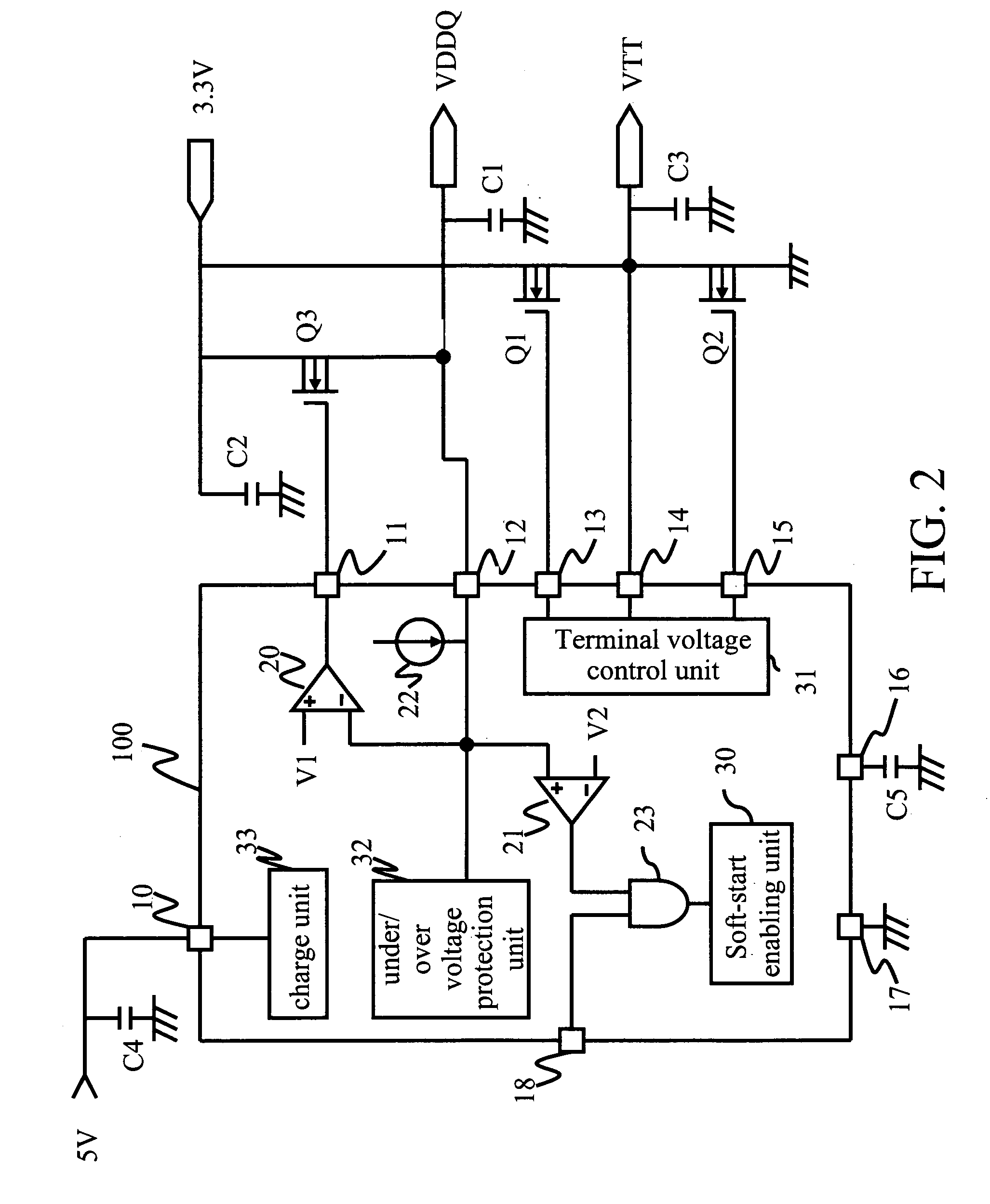
[0029]With reference to FIG. 2, a system block diagram of the power supply chip of the present invention is disclosed, which comprises a first voltage comparator unit 20, a third transistor switch Q3, a second voltage comparator unit 21, a current source unit 22, an arithmetic logic unit 23, a soft start enabling unit 30 and a terminal voltage control unit 31.

[0030]The first voltage comparator unit 20 which may be constituted of a comparator used for comparing the reference voltage signal V1 and the voltage level formed by the first capacitor C1 so as to output a first drive signal, in which the first input end receives a reference voltage signal V1, and the second input end is connected to the under / over voltage protection unit 32.

[0031]The third transistor switch Q3, which may be constituted of the NMOS (N-type metal-oxide semiconductor) transistor switch or the PMOS (P-type metal-oxide semiconductor) transistor switch, is triggered to be on by the first drive signal and will be i...


PUM


Abstract

A dual loop voltage regulation circuit of power supply chip is provided, comprising a capacitor for providing a voltage signal, a comparator for comparing a first reference voltage signal and the voltage signal to output forward or backward trigger signal, a first switch triggered by a forward trigger signal, a second switch triggered by a backward trigger signal, a first operational amplifier generating a first drive signal while the first and second switches are on, a first transistor switch triggered to be on by a first drive signal to provide a current source loop, a third switch triggered by a forward trigger signal, a fourth switch triggered by a backward trigger signal, a second operational amplifier generating a second drive signal while the third and fourth switches are on, and a second transistor switch triggered to be on by a second drive signal to provide a current sink loop.

Description

[0001]This Non-provisional application claims priority under 35 U.S.C. § 119(a) on Patent Application No(s). 094121919 filed in Taiwan on Jun. 29, 2005, the entire contents of which are hereby incorporated by reference.BACKGROUND OF THE INVENTION[0002]1. Field of Invention[0003]The present invention relates to a voltage regulation circuit, and more particularly to a dual loop voltage regulation circuit of power supply chip.[0004]2. Related Art[0005]Generally, a conventional system of a voltage regulation circuit of current source and current sink is a single close loop system. Due to the use of the single close loop system, there is a need for a relatively large offset voltage to control the output of one of the amplifiers to be high potential, resulting in an overtime of the non-overlap, which makes the output voltage dithering easily. Referring to FIG. 1, a circuit diagram of a conventional voltage regulation circuit is illustrated, when an output voltage (V0*R2) / (R1+R2) is lower ...

Claims


Application Information

Patent Timeline
Patent Type & Authority Patents(United States)
IPC IPC(8): G05F1/10
CPCH03K17/165H03K17/04206
Inventor WEI, DA-CHUNCHIA, JU-LINCHU, YI-SHAN
Owner LEADTREND TECH
Why Eureka
Try Eureka