Stacked organic photosensitive devices

a photosensitive device and organic technology, applied in the direction of semiconductor devices, electrical equipment, nanotechnology, etc., can solve the problems of difficult and expensive production of efficient crystalline-based devices, not providing a signal or current to control detection circuitry, not providing power to devices, equipment, circuitry,

Active Publication Date: 2007-03-27
THE TRUSTEES FOR PRINCETON UNIV
View PDF18 Cites 51 Cited by
  • Summary
  • Abstract
  • Description
  • Claims
  • Application Information

AI Technical Summary

Problems solved by technology

As a general rule, a photovoltaic cell provides power to a circuit, device or equipment, but does not provide a signal or current to control detection circuitry, or the output of information from the detection circuitry.
In contrast, a photodetector or photoconductor provides a signal or current to control detection circuitry, or the output of information from the detection circuitry but does not provide power to the circuitry, device or equipment.
However, efficient crystalline-based devices, especially of large surface area, are difficult and expensive to produce due to the problems inherent in producing large crystals without significant efficiency-degrading defects.
On the other hand, high efficiency amorphous silicon devices still suffer from problems with stability.
The maximum total power generated by a PV device is inherently incapable of exceeding the product, ISC×VOC.
Either of these outcomes is undesirable in a photosensitive optoelectronic device.
Such a process can be induced by the built-in electric field, but the efficiency at the electric fields typically found in organic devices (F˜106 V / cm) is low.
However, some organic PV devices typically have relatively low external quantum efficiency, being on the order of 1% or less.
In this process energy is lost which will result in a lower efficiency for the device.

Method used


Image

  • Stacked organic photosensitive devices
  • Stacked organic photosensitive devices
  • Stacked organic photosensitive devices

Examples


examples

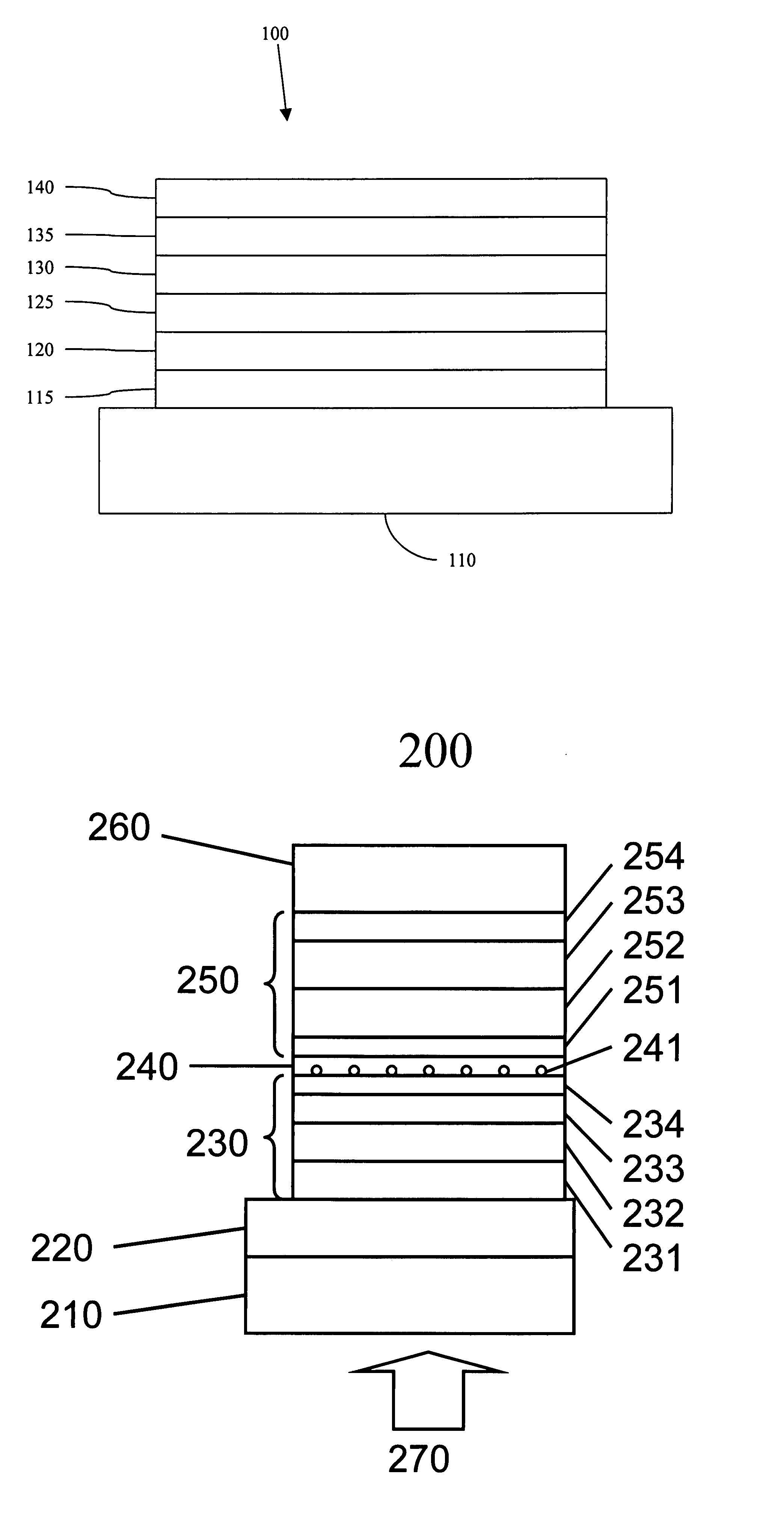
[0104]In one embodiment of the invention, an efficient photovoltaic cell is provided. A cell with two stacked hybrid planar-mixed heterojunction cells was fabricated on a glass substrate pre-coated with transparent conducting ITO. The device has the structure: ITO / 75 Å CuPc / 122 Å CuPc:C60 (1.2:1 by weight) / 80 Å C60 / 50 Å PTCBI / 5 Å Ag / 50 Å m-MTDATA:F4-TCNQ / 60 Å CuPc / 132 Å CuPc:C60 (1.2:1 by weight) / 160 Å C60 / 75 Å BCP / Ag. The cell farther away from the cathode is slightly rich in CuPc, which absorbs in the spectral region from 550 nm to 750 nm, whereas the cell closer to the cathode is rich in C60, which absorbs in the spectral region from 350 nm to 550 nm. A maximum power efficiency was measured of (5.6±0.3)% under 1 to 4 suns simulated AM1.5G solar illumination.

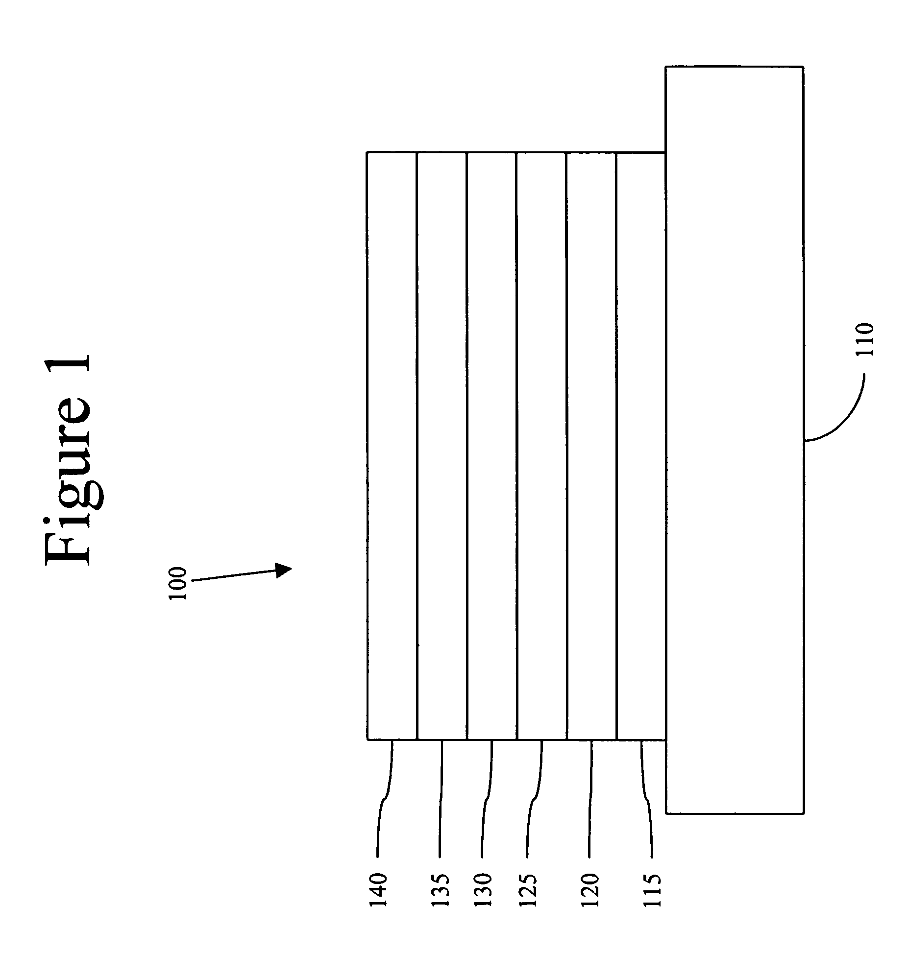
[0105]The organic hybrid planar-mixed heterojunction photovoltaic cells were fabricated on glass substrates precoated with a ˜1500 Å thick transparent, conducting ITO anode with a sheet resistance of 15 Ω / sq. The substrates we...


PUM


Abstract

A device is provided having a first electrode, a second electrode, a first photoactive region having a characteristic absorption wavelength λ1 and a second photoactive region having a characteristic absorption wavelength λ2. The photoactive regions are disposed between the first and second electrodes, and further positioned on the same side of a reflective layer, such that the first photoactive region is closer to the reflective layer than the second photoactive region. The materials comprising the photoactive regions may be selected such that λ1 is at least about 10% different from λ2. The device may further comprise an exciton blocking layer disposed adjacent to and in direct contact with the organic acceptor material of each photoactive region, wherein the LUMO of each exciton blocking layer other than that closest to the cathode is not more than about 0.3 eV greater than the LUMO of the acceptor material.

Description

UNITED STATES GOVERNMENT RIGHTS[0001]This invention was made with U.S. Government support under Contract No. 341-4141 awarded by U.S. Department of Energy, National Renewable Energy Laboratory. The government has certain rights in this invention.JOINT RESEARCH AGREEMENT[0002]The claimed invention was made by, on behalf of, and / or in connection with one or more of the following parties to a joint university-corporation research agreement: Princeton University, The University of Southern California, and Global Photonic Energy Corporation. The agreement was in effect on and before the date the claimed invention was made, and the claimed invention was made as a result of activities undertaken within the scope of the agreement.FIELD OF THE INVENTION[0003]The present invention generally relates to organic photosensitive optoelectronic devices. More specifically, it is directed to organic photosensitive optoelectronic devices having increased efficiency.BACKGROUND OF THE INVENTION[0004]Opt...

Claims


Application Information

Patent Timeline
Patent Type & Authority Patents(United States)
IPC IPC(8): H01L31/062
CPCB82Y10/00H01L27/302H01L51/0021H01L51/4246H01L51/4253H01L51/0046Y02E10/549H01L51/0059H01L51/0078H01L51/0053H10K30/57H10K71/60H10K85/211H10K85/621H10K85/311H10K85/631H10K30/211H10K30/30H01L31/04H10K30/00
Inventor FORREST, STEPHENXUE, JIANGENGUCHIDA, SOICHIRAND, BARRY P.
Owner THE TRUSTEES FOR PRINCETON UNIV
Why Eureka
Try Eureka