ESD protection apparatus for an electrical device

a protection apparatus and electrical device technology, applied in electrical devices, semiconductor devices, semiconductor/solid-state device details, etc., can solve the problems of current and voltage flow at the inputs, and the curves of current and voltage flow are flattening, so as to reduce the effect of reducing the input and output capacitance and reducing the capacitan

Inactive Publication Date: 2007-03-27
POLARIS INNOVATIONS
View PDF12 Cites 11 Cited by
  • Summary
  • Abstract
  • Description
  • Claims
  • Application Information

AI Technical Summary

Benefits of technology

[0017]The present invention is based on the knowledge that part of the ESD event current can be drained by a gas discharge, so that a current through the ESD protection diode can be made smaller.
[0018]An ESD protection structure according to an embodiment of the present invention can be designed in order to have a lower capacitance than only an ESD protection diode. This allows the reduction of an input and an output capacitance, respectively, applied to a chip pad, whereby data rates of a higher frequency can be transmitted via the respective chip pad.
[0019]Above that, the ESD protection structure according to an embodiment of the present invention allows to embody the ESD protection diode for an overload current in a chip connected thereto. This is accompanied by an area reduction of the chip. Thereby, the chip can be produced at lower cost, wherein at the same time the yield in production increases with decreasing chip area.
[0020]In a device according to the present invention using an ESD protection apparatus according to an embodiment of the present invention and wherein additionally an ESD protection diode is attached to the internal terminal at the circuit structure, the ESD protection diode can be made with a significantly reduced area compared to the prior art. A portion of an occurring overvoltage can thereby be intercepted and limited at the ESD protection apparatus, while only a remaining low portion is accommodated by the ESD protection diode whose area can thus be smaller. The reduction of the area of the ESD protection diode is thereby accompanied by a decrease of capacitance of the ESD protection diode.

Problems solved by technology

These capacities do lead to a flattening of the curves of the current and voltage flows at the inputs and outputs of the integrated circuit.

Method used


Image

  • ESD protection apparatus for an electrical device
  • ESD protection apparatus for an electrical device

Examples


Embodiment Construction

[0036]In the following description, the same or similar elements are provided with the same reference numbers.

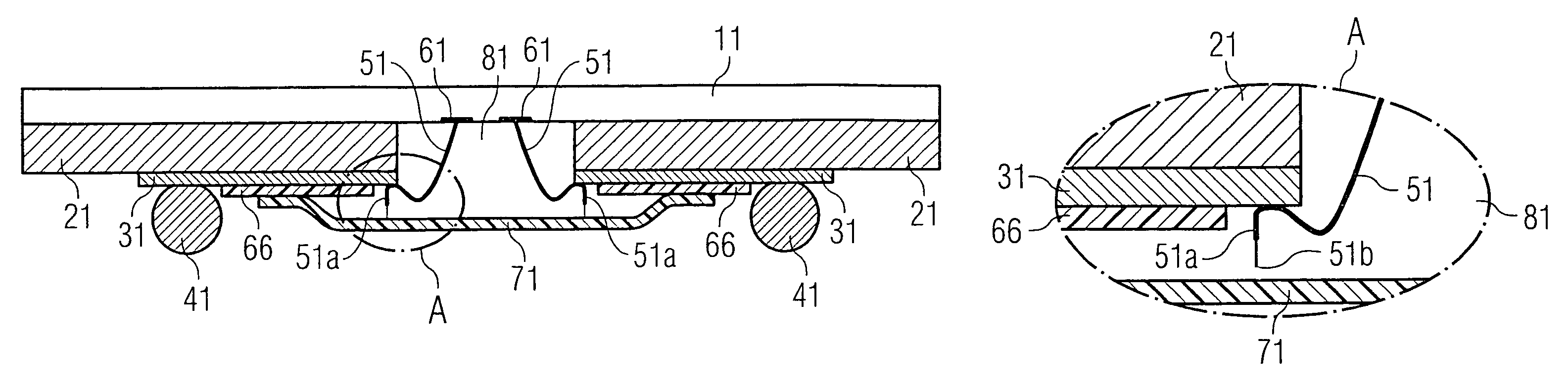
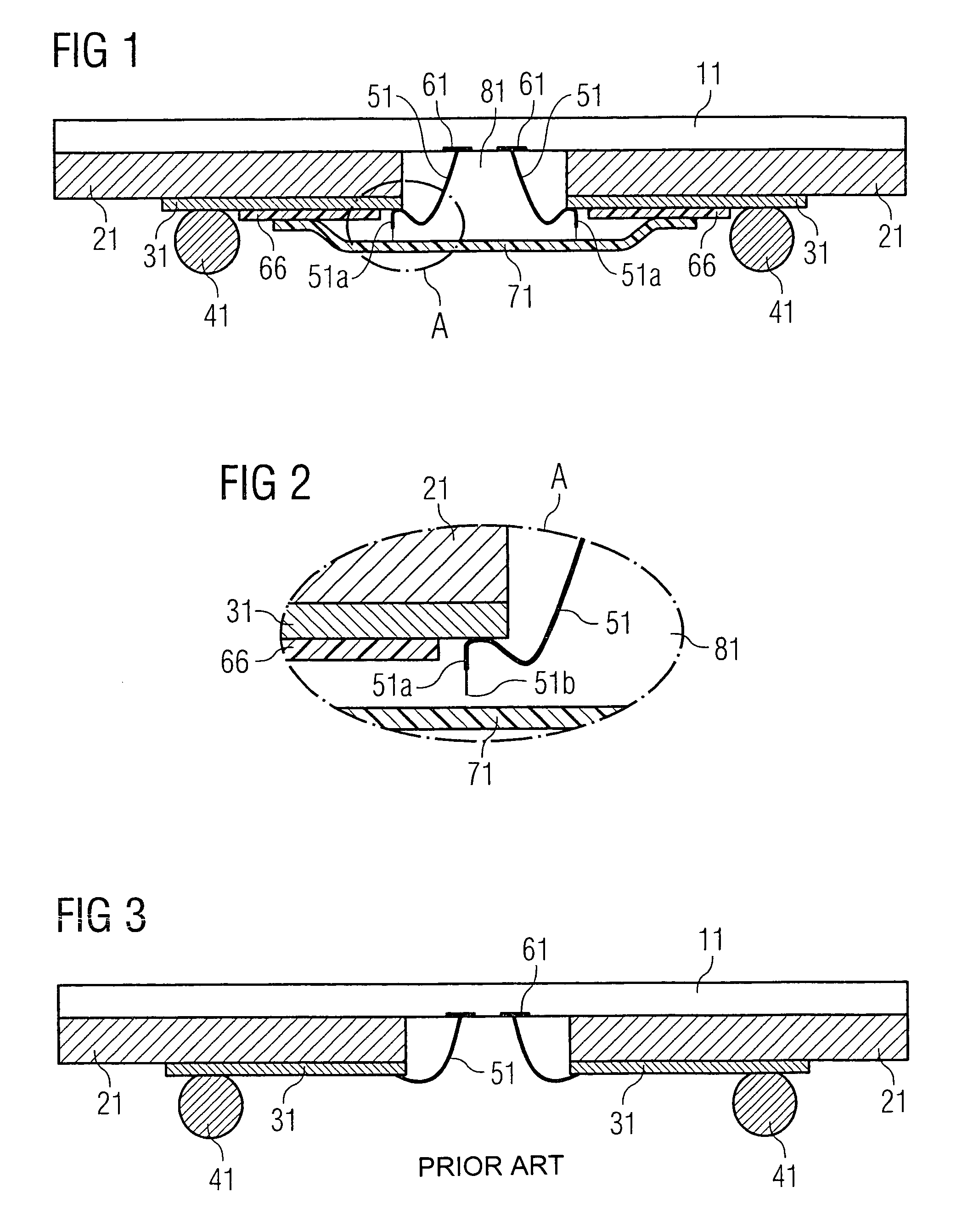
[0037]FIG. 1 shows a structure of a BGA package with an ESD protection apparatus according to an embodiment of the present invention. The structure of the BGA package without ESD protection apparatus corresponds to the one described with reference to FIG. 3, so that a repeated illustration is omitted.

[0038]Additionally, in FIG. 1, compared with FIG. 3, bond wire ends 51a, an isolation layer 66 and a cover 71 are shown.

[0039]Here, the ESD protection apparatus is formed of the bond wire ends 51a disposed on the traces 31. These extend in the direction of a cover 71 disposed on an isolation layer 66. Thereby, a rare gas 81 is filled in the cavity formed of a chip 11, the package substrate 21, the traces 31, the isolation layers 66 and the cover 71.

[0040]Thereby, the cavity is substantially closed gas-tight, so that the rare gas 81 cannot leak out therefrom. The bond wires 51 be...


PUM


Abstract

An ESD protection apparatus for an electrical device with a circuit structure having an internal terminal, which is connected to an external terminal of the electrical device via a conductive connection, has a gas-filled cavity, through which the conductive connection extends at least partly, and a reference electrode in the cavity, wherein the conductive connection is disposed such in the cavity, that when applying a potential exceeding a predetermined threshold to the external terminal, a gas discharge occurs from the conductive connection to the reference electrode.

Description

BACKGROUND OF THE INVENTION[0001]1. Field of the Invention[0002]The present invention relates to an ESD protection apparatus for an electrical device.[0003]2. Description of the Related Art[0004]In microelectronics, more and more integrated circuits with low structure widths are utilized. These lower structure widths enable higher clock rates of the integrated circuits and thus higher data rates of the signals at the pins of the integrated circuits. In order to enable a communication between two electrical devices, which is as interference-free as possible, it is required to make the leading and falling edges of the transmitted bits as steep as possible. Therefore, it is required to keep the capacitive loads at the inputs and outputs of an integrated circuit as low as possible. These capacities do lead to a flattening of the curves of the current and voltage flows at the inputs and outputs of the integrated circuit.[0005]An integrity of the signal in modern integrated circuits depen...

Claims


Application Information

Patent Timeline
Patent Type & Authority Patents(United States)
IPC IPC(8): H01L23/20H01L23/22H01L23/24H01L23/34H01L23/62
CPCH01L23/60H01L24/73H01L2924/01002H01L2924/01023H01L2924/0102H01L2924/01029H01L2924/01054H01L2924/01078H01L2924/01082H01L2924/14H01L2924/15311H01L2924/19041H01L2924/30107H01L2924/3025H01L2924/1301H01L2224/73215H01L2224/48091H01L2224/48237H01L2224/4826H01L24/48H01L2924/01005H01L2924/0101H01L2924/00014H01L2924/00H01L2224/4824
Inventor KUZMENKA, MAKSIM
Owner POLARIS INNOVATIONS
Why Eureka
Try Eureka