Latch circuit, shift register circuit, logical circuit and image display device operated with a low consumption of power

a shift register and logical circuit technology, applied in logic circuit coupling/interface arrangement, instruments, pulse techniques, etc., can solve problems such as power increase in external circuits, troublesome occurrence of display image ghosting, and above-mentioned liquid crystal display devices, so as to reduce capacitive load, increase operating margin, and reduce power consumption

Inactive Publication Date: 2007-03-27
SHARP KK
View PDF24 Cites 37 Cited by
  • Summary
  • Abstract
  • Description
  • Claims
  • Application Information

AI Technical Summary

Benefits of technology

[0022]Accordingly, the object of the present invention is to provide a shift register circuit of which the load of the clock signal line and the consumption of power are reduced to concurrently achieve a low-voltage interface and a low consumption of power with a boosting function incorporated in the latch circuit as well as an image display device that employs this shift register circuit and concurrently has a low consumption of power and a high display quality.

Problems solved by technology

However, the aforementioned conventional liquid crystal display device has the problems as follows.
In such a case, a noise is imposed on the data signal line SL, leading to a concern about the occurrence of troubles such as blur, ghost and crosstalk of the display image.
However, if the clock signals cks and ckg have an increased amplitude, then there occurs the problem that the consumption of power increases in the external circuits such as a control circuit (not shown) for generating the clock signal and the like.
Furthermore, unwanted emission from the signal lines becomes a serious problem.
Furthermore, since the driving capability of the level shifter circuit LS itself is low, there is necessitated a buffer for driving the subsequent signal lines, also causing the problem that the consumption of power increases.
This causes another problem that the transistors have an increased gate area and the consequent increase in load and consumption of power of the clock signal line.

Method used


Image

  • Latch circuit, shift register circuit, logical circuit and image display device operated with a low consumption of power
  • Latch circuit, shift register circuit, logical circuit and image display device operated with a low consumption of power
  • Latch circuit, shift register circuit, logical circuit and image display device operated with a low consumption of power

Examples


first embodiment

[0449]A first embodiment of the logical circuit of the present invention will be described below with reference to drawings. FIG. 51 is a block diagram showing an example of the construction of the logical circuit according to the present invention. In FIG. 51, the drive voltage of the logical circuit is 15 V, and the amplitude of each of input signals IN2 and / IN2 is 15 V, whereas the amplitude of each of input signals IN1 and / IN1 is 5 V.

[0450]In the logical circuit of the present invention, by inputting the input signal having a lower voltage than the drive voltage to the logical circuit, it is possible to reduce the power consumption of an input signal line.

[0451]Referring to FIG. 51, the amplitude of each of the input signals IN2 and / IN2 is different from that of each of the input signals IN1 and / IN1. However, there is no problem when the amplitude of each of the input signals IN2 and / IN2 and that of each of the input signals IN1 and / IN1 are equally 5 V. This applies to the...

second embodiment

[0462]A second embodiment of the logical circuit of the present invention will be described below with reference to drawings.

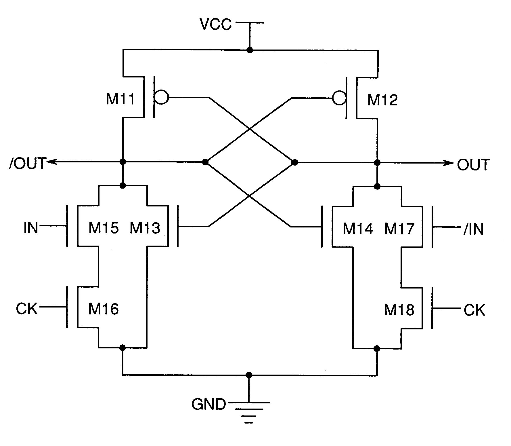
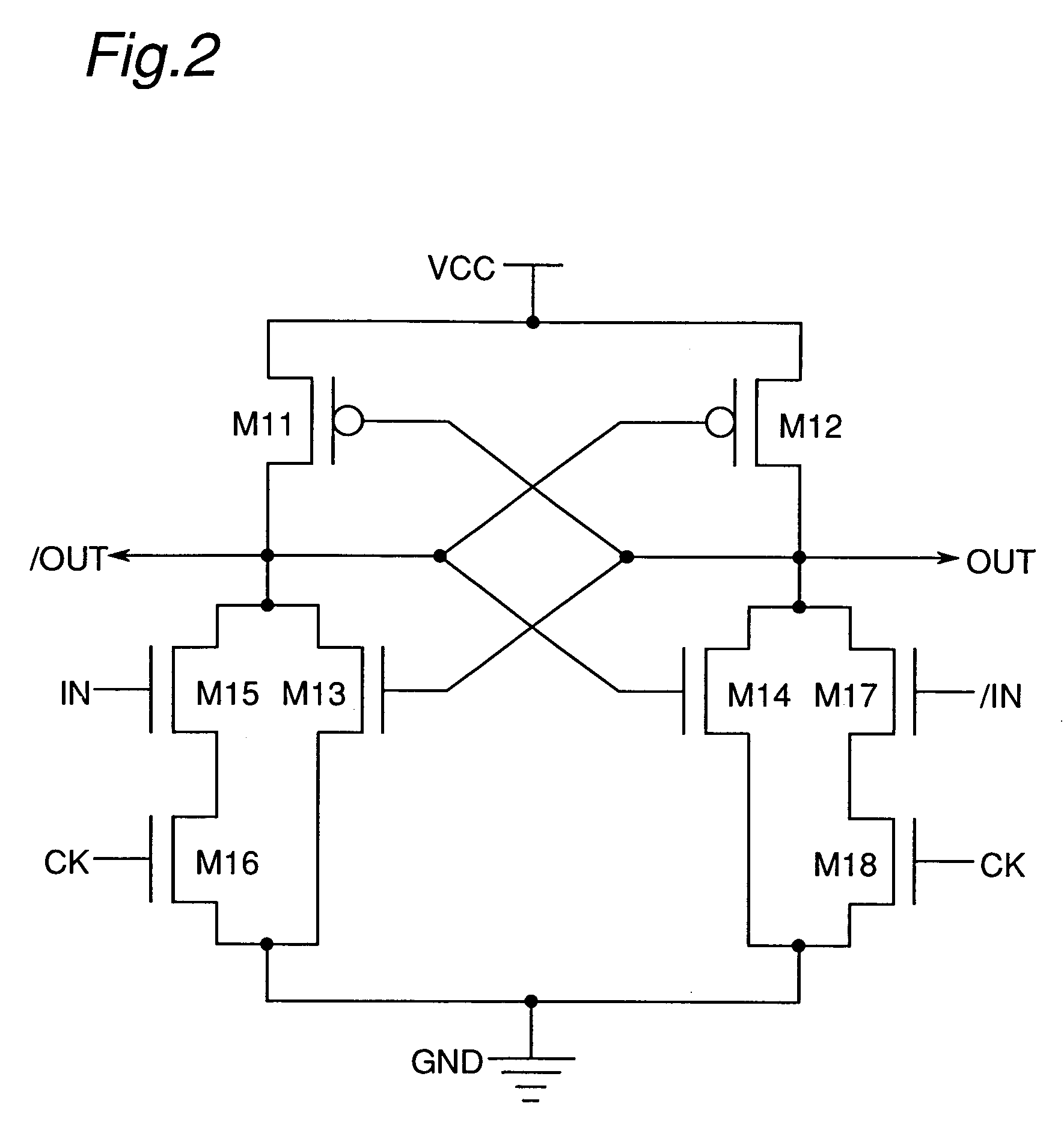
[0463]FIG. 58 is a circuit diagram showing an example of the construction of the logical circuit according to the present invention. The circuit has the function of a non-conjunction (NAND) circuit. But depending on a signal selection manner of input and out put, the circuit can serve as any of a non-disjunction (NOR) circuit, logical product (AND) circuit, and a logical sum (OR) circuit. That is, supposing that input signals to the logical circuit are IN1 and IN2 and that an output signal therefrom is / OUT, the logical circuit functions as the non-conjunction circuit. Supposing that the input signals thereto are / IN1 and / IN2 and that the output signal therefrom is OUT, the logical circuit functions as the non-disjunction circuit. Further, supposing that the input signals thereto are IN1 and IN2 and that the output signal therefrom is OUT, the logical circuit...

third embodiment

[0467]Another embodiment of the logical circuit of the present invention will be described below with reference to drawings. FIGS. 59 and 60 are circuit diagrams showing another example of the construction of the logical circuit of the present invention.

[0468]The circuit has the function of a logical product and non-disjunction (AND-NOR) circuit. But depending on a signal selection manner of input and output, the circuit can serve as any of a logical sum and non-conjunction (OR-NAND) circuit, a logical product-logical sum (AND-OR) circuit, a logical sum-logical product (OR-AND) circuit. That is, supposing that input signals to the logical circuit are IN1, IN2, and IN3 and that an output signal therefrom is / OUT, the logical circuit functions as the logical product and non-disjunction circuit. Supposing that the input signals thereto are / IN1, / IN2, and / IN3 and that the output signal therefrom is OUT, the logical circuit functions as the logical sum and non-conjunction circuit. Furt...


PUM


Abstract

A CMOS logical circuit comprises two electric current paths each of which has circuits consisting of n-type and p-type transistors. In a circuit consisting of n-type or p-type transistors, one electric current path is provided with a circuit having the same construction as that of a circuit having an n-type transistor of a CMOS logical circuit outputting a logical operation result similar to that of this logical circuit, and the other electric current path is provided with a circuit having the same construction as that of a circuit having a p-type transistor of the CMOS logical circuit outputting a logical operation result similar to that of this logical circuit. In another circuit consisting of the other channel type, a gate electrode of the transistor provided on the one electric current path and that of the transistor provided on the other electric current path are connected to drain electrodes of the counterparts. According to the construction, the amplitude of an input signal can be made smaller than a supply voltage of the logical circuit.

Description

CROSS-REFERENCE TO RELATED APPLICATION(S)[0001]This application is a continuation-in-part of copending application U.S. Ser. No. 09 / 300,178, filed on Apr. 27, 1999.BACKGROUND OF THE INVENTION[0002]The present invention relates to a latch circuit for transmitting a pulse signal, a shift register circuit having this latch circuit and an image display device employing this shift register circuit, as well as a logical circuit for performing a logical operation of an input signal capable of performing a normal logical operation of an input signal having a smaller amplitude than a supply voltage of the logical circuit.[0003]Herein is provided a description for a conventional liquid crystal display device and a shift register circuit that constitutes the data signal line drive circuit and scanning signal line drive circuit of the device, which are taken as examples of an image display device and a shift register circuit having the conventional latch circuit. It is to be noted that the shif...

Claims


Application Information

Patent Timeline
Patent Type & Authority Patents(United States)
IPC IPC(8): G09G5/00G09G3/26H03K19/00H03K19/0175H03K5/153
CPCG09G3/3677G09G3/3688G11C19/28G11C19/00G09G2300/0408G09G2300/0417G09G2310/0289G09G2330/021G09G2310/021
Inventor KUBOTA, YASUSHIWASHIO, HAJIMESHIRAKI, ICHIROMAEDA, KAZUHIROKAISE, YASUYOSHI
Owner SHARP KK
Why Eureka
Try Eureka