Stacked DRAM memory chip for a dual inline memory module (DIMM)

a dual-in-line memory module and memory chip technology, applied in the field of stacked dram memory chips for dual-in-line memory modules, can solve the problems of increasing the load of the dq-data bus, limiting the number of memory ranks, and deteriorating the load connected to each dq-data bus

Active Publication Date: 2007-04-03
POLARIS INNOVATIONS LTD
View PDF2 Cites 232 Cited by
  • Summary
  • Abstract
  • Description
  • Claims
  • Application Information

AI Technical Summary

Benefits of technology

[0017]Accordingly it is the object of the present invention to provide a stacked DRAM memory chip for a Dual Inline Memory Module allowing for a predetermined operation frequency an increased number of memory ranks on the Dual Inline Memory Module.
[0029]This has the advantage that by integrating the memory rank decoder within the DRAM memory chip the number of selection signals which have to be supplied by the command and address buffer to each DRAM chip is reduced. Consequently the number of selection signal lines on the Dual Inline Memory Module is reduced so that the size of the printed circuit board is decreased and the complexity of the line routing is diminished.

Problems solved by technology

The increase of memory ranks on the Dual Inline Memory Module however causes an increase of the load of the DQ-data bus which is driven by the controller on the motherboard.
Consequently an increase of the load connected to each DQ data bus deteriorates rates the data signals further so that data errors can not be excluded.
Accordingly there is a limitation of the number M of memory ranks within a DRAM chip connected to the DQ-bus of said chip.
By limiting the number of memory ranks allowed within a DRAM chip the memory capacity of a Dual Inline Memory is also limited.

Method used


Image

  • Stacked DRAM memory chip for a dual inline memory module (DIMM)
  • Stacked DRAM memory chip for a dual inline memory module (DIMM)
  • Stacked DRAM memory chip for a dual inline memory module (DIMM)

Examples


Embodiment Construction

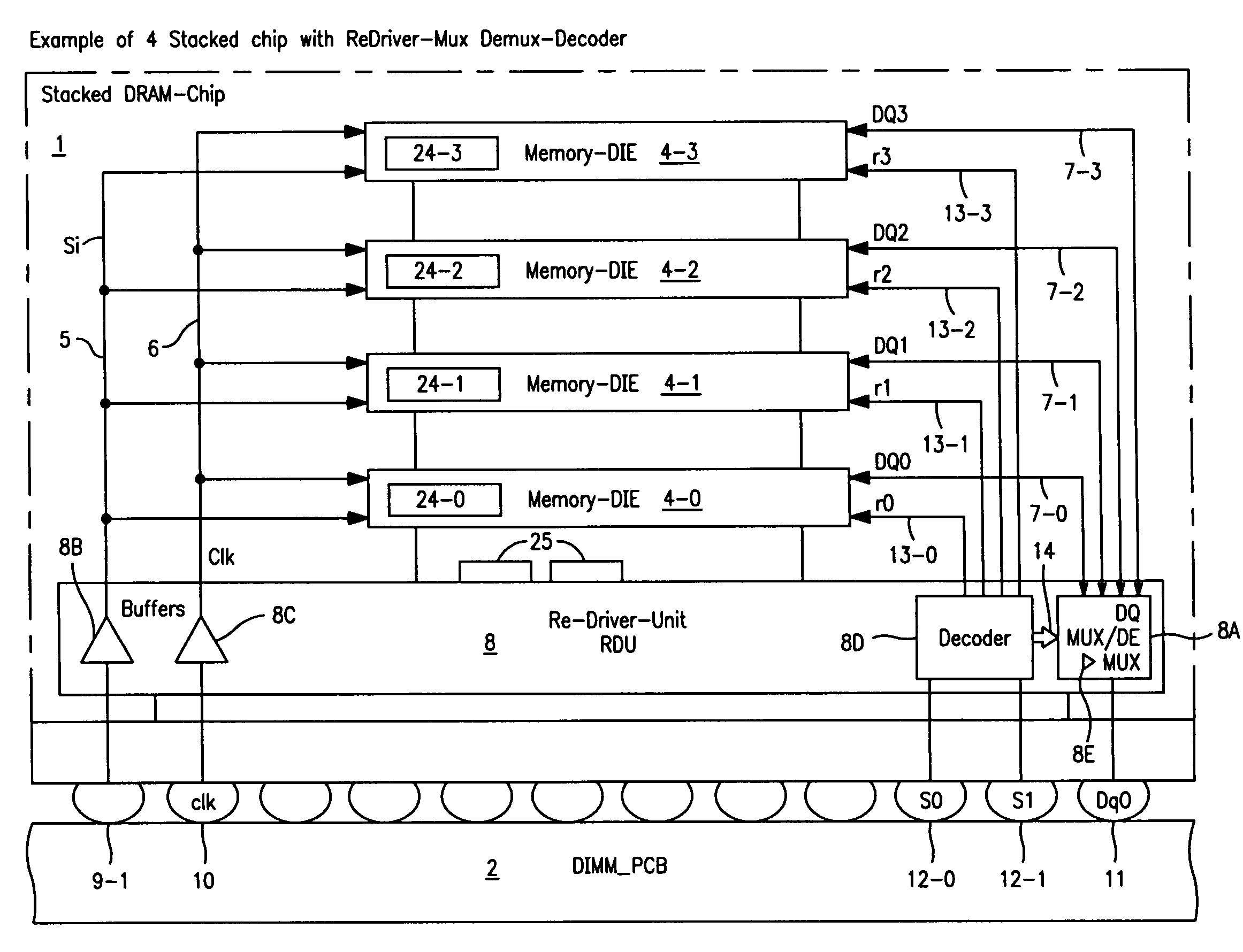
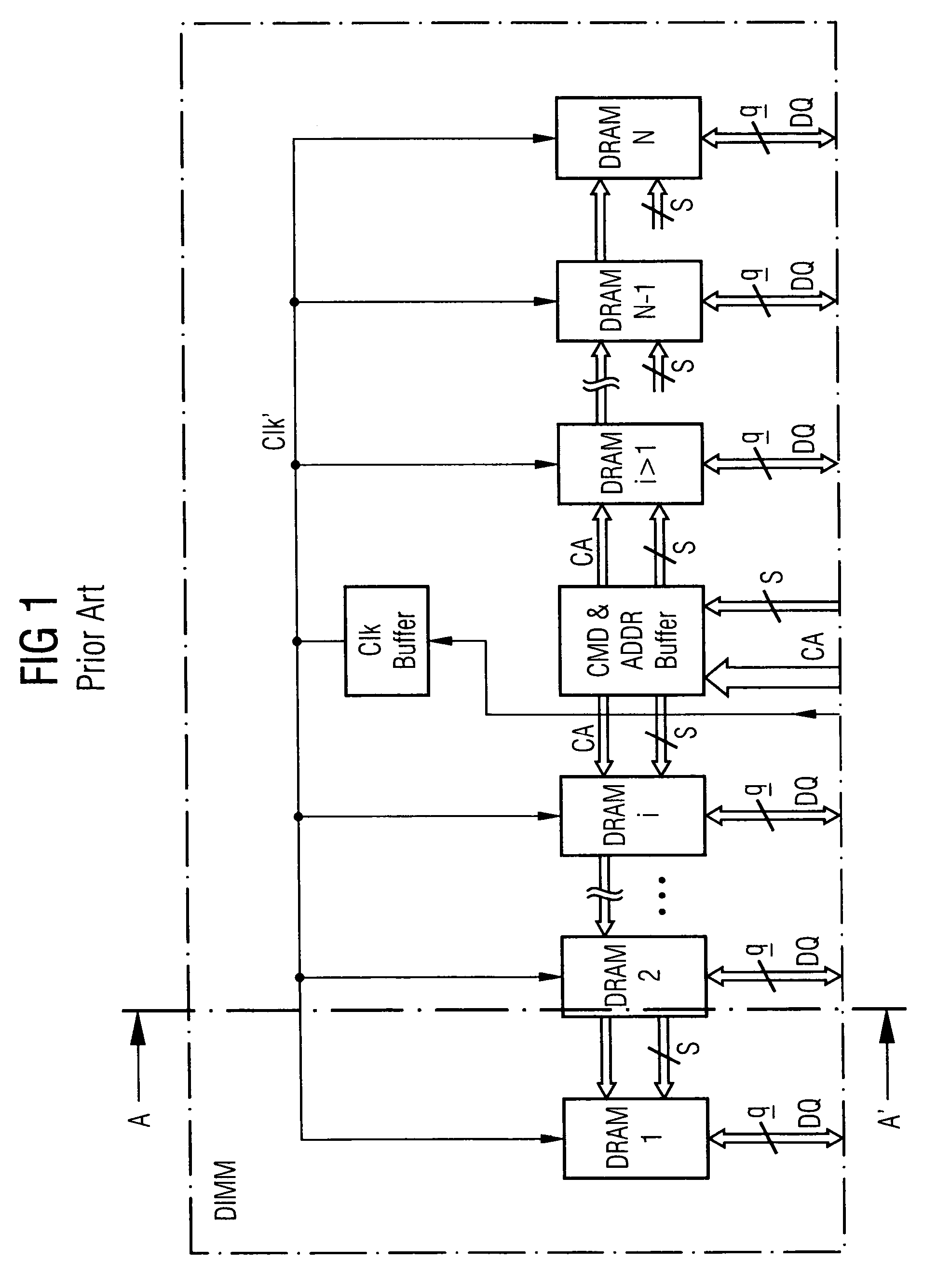
[0053]Referring to FIG. 4 it shows a cross section of a stacked DRAM memory chip 1 mounted on a printed circuit board (PCB) 2 of a Dual Inline Memory Module 3 (shown in FIG. 5). The stacked DRAM chip I as shown in FIG. 4 comprises in the shown embodiment four stacked DRAM memory dies 4-0, 4-1, 4-2, 4-3. Each memory die 4-i is selectable by a corresponding memory rank signal r–i. The DRAM memory dies 4-i include an array of memory cells (designated 24-0. 24-1. 24-2. and 24-3) which are addressable by address lines. A common internal address bus 5 comprises a predetermined number of internal address lines 5-i provided for addressing memory cells 24-i of the memory dies 4-i. FIG. 4 shows as an example an address pad A0 connected via an address line 5-i to all memory dies 4-i. All address lines of the internal address bus are connected in parallel to all four DRAM memory dies of the stacked DRAM chip 1. The memory dies 4-i are clocked by a clock signal CLK applied to all memory dies via...


PUM


Abstract

A stacked DRAM memory chip for a Dual In Line Memory Module (DIMM) is disclosed. According to one aspect, the DRAM memory chip comprises at least four stacked DRAM memory dies. Further, the memory dies are each selectable by a corresponding internal memory rank signal. Each memory die comprises an array of memory cells. A common internal address bus is provided for addressing the memory cells and is connected to all stacked DRAM memory dies. Internal data buses are provided for writing data into the memory cells and reading data out of the memory cells of the DRAM memory dies. An integrated redriving unit comprises buffers for all internal address lines provided for driving external address signals applied to address pads of the DRAM memory chip. A multiplexer / demultiplexer switches the internal data lines of the selected DRAM memory die. A memory rank decoder selects a corresponding memory die.

Description

TECHNICAL FIELD[0001]The invention relates in general to a DRAM chip for a DRAM Dual Inline Memory Module (DIMM) and in particular to a DRAM memory chip for a registered Dual Inline Memory Module (DIMM).BACKGROUND ART[0002]Memory modules are provided for increasing the memory capacity of a computer system. Originally single inline memory modules (SIMM) were used in personal computers to increase the memory size. A single inline memory module comprises DRAM chips on its printed circuit board (PCB) only on one side. The contacts for connecting the printed circuit board of the single inline memory module (SIMM) are redundant on both sides of the module. A first variant of SIMMs has thirty pins and provides 8 bits of data (9 bits in parity versions). A second variant of SIMMs which are called PS / 2 comprise 72 pins and provide 32 bits of data (36 bits in parity versions).[0003]Due to the different data bus width of the memory module in some processors, sometimes several SIMM modules are ...

Claims


Application Information

Patent Timeline
Patent Type & Authority Patents(United States)
IPC IPC(8): G11C5/02
CPCB82Y10/00G11C5/04H01L25/0657H01L25/18H01L2224/48091H01L2224/48227H01L2225/0651H01L2225/06524H01L2225/06527H01L2924/0102H01L2924/01078H01L2924/15311H01L2924/00014H01L2924/01068
Inventor RAGHURAM, SIVA
Owner POLARIS INNOVATIONS LTD
Why Eureka
Try Eureka