Error-checking and correcting decryption-key memory for programmable logic devices

a programmable logic and decryption key technology, applied in the direction of unauthorized memory use protection, pulse technique, instruments, etc., can solve the problems of design effort being copied by someone else, design implementation in plds is so complex, and it takes months to complete and debug a design to be implemented,

Active Publication Date: 2007-04-03
XILINX INC
View PDF65 Cites 92 Cited by
  • Summary
  • Abstract
  • Description
  • Claims
  • Application Information

AI Technical Summary

Benefits of technology

[0020]Another embodiment further protects decryption keys by encrypting the keys themselves before transferring them to a key memory in the target PLD, thus ensuring the keys will not be compromised in transit. One such embodiment encrypts a decryption key for decrypting configuration data (the “configuration key”) using a Public-Key Encryption algorithm (e.g., RSA). The configuration key is encrypted using a public key prior to transfer to the PLD. Once in the PLD, the configuration key is decrypted using a private key previously stored on the PLD. The decryptor used to decrypt the configuration key can be instantiated on the PLD using programmable resources.
[0021]Another embodiment includes a PLD in which the key memory can be operated in a secure mode or a non-secure mode. The non-secure mode allows the decryption keys to be read or written freely; the secure mode bars read and write access to the decryption keys. The PLD supports secure and non-secure modes on a key-by-key basis. Users may therefore write, verify, and erase individual keys without affecting others.

Problems solved by technology

Designs implemented in PLDs have become so complex that it often takes months to complete and debug a design to be implemented in a PLD.
When the design is going into a system of which the PLD is a part and is to be sold for profit, the designer does not want the result of this design effort to be copied by someone else.
Since configuration data is stored external to the PLD and must be transmitted through a configuration access port, the privacy of the design can easily be violated by an attacker who monitors the data on the configuration access port, e.g. by putting probes on board traces.
Efforts have been made to encrypt designs, but it is difficult to make the design both secure from attackers and easy to use by legitimate users.
However, power and system cost requirements make this method impractical for many applications.
If the design is loaded at the factory before the device is sold, it is difficult for a purchaser of the configured PLD device to determine what the design is.
Some memory technologies, such as antifuses, are vulnerable to inspection under a microscope.
Also disadvantageous, nonvolatile memory fabrication requires a more complex and more expensive process technology than standard CMOS process technology, and takes longer to bring to market.
However, these arrangements do not protect user's designs from all modes of attack.

Method used


Image

  • Error-checking and correcting decryption-key memory for programmable logic devices
  • Error-checking and correcting decryption-key memory for programmable logic devices
  • Error-checking and correcting decryption-key memory for programmable logic devices

Examples


Embodiment Construction

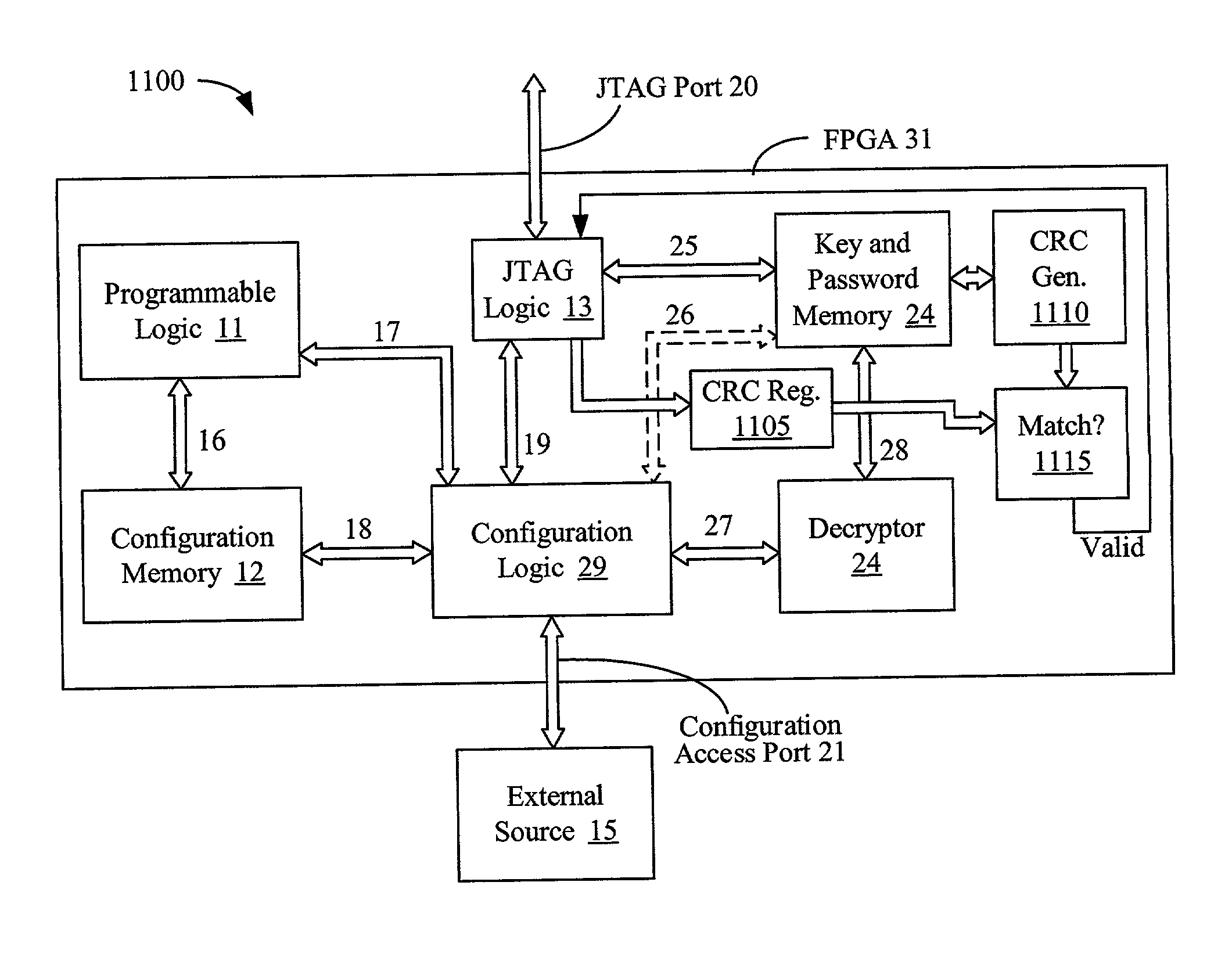
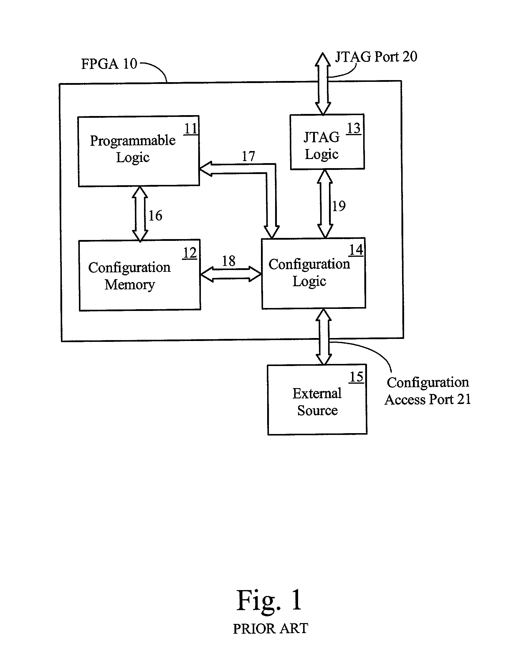
[0047]FIG. 1 shows a prior art structure for an FPGA 10. The FPGA includes programmable logic 11, typically comprising (1) logic blocks with lookup-table combinational logic function generators, flip-flops for storing lookup table outputs and other values, and multiplexers and logic gates for enhancing the logic ability of the programmable logic (2) routing lines and programmable interconnection points for routing signals around the FPGA, and (3) input / output blocks for driving signals between the routing lines and the external pins of the FPGA. The above-listed elements are not shown here, but are described by Young in U.S. Pat. No. 5,933,023, entitled “FPGA Architecture Having RAM Blocks with Programmable Word Length and Width and Dedicated Address and Data Lines”, which is incorporated herein by reference.

[0048]The FPGA also includes configuration memory 12 for turning on routing transistors, controlling multiplexers, storing lookup tables, and controlling the input / output blocks...


PUM


Abstract

Described are circuits that detect and correct for decryption key errors. In one example, a programmable logic device includes a decryption key memory with a number of decryption-key fields and, for each key field, an associated error-correction-code (ECC) field. The PLD additionally includes error-correction circuitry that receives each key and associated ECC and performs an error correction before conveying the resulting error-corrected key to a decryptor.

Description

[0001]This is a divisional application to the U.S. patent application Ser. No. 10 / 112,790, filed Mar. 29, 2002 which is currently pending.BACKGROUND[0002]A PLD (programmable logic device) is an integrated circuit that performs digital logic functions selected by a designer. PLDs include logic blocks and interconnect lines, and typically both the logic blocks and interconnect lines are programmable. One common type of PLD is an FPGA (field programmable gate array), in which the logic blocks typically include lookup tables and flip-flops that generate and store any logic function of their input signals. Another type of PLD is the CPLD (complex programmable logic device), in which the logic blocks perform the AND function and the OR function and the selection of input signals is programmable.[0003]Designs implemented in PLDs have become so complex that it often takes months to complete and debug a design to be implemented in a PLD. When the design is going into a system of which the PL...

Claims


Application Information

Patent Timeline
Patent Type & Authority Patents(United States)
IPC IPC(8): H04L9/14H04L1/00
CPCG06F12/1425G06F21/57G06F21/79G06Q20/3829H04L9/0637H04L9/0897H04L2209/34
Inventor TRIMBERGER, STEPHEN M.
Owner XILINX INC
Why Eureka
Try Eureka