Semiconductor device

a semiconductor and device technology, applied in semiconductor devices, instruments, electrical devices, etc., can solve problems such as display failure, loss of light shutter function, and rubbing failure, and achieve the effect of effective filling and flattening unevenness and enhancing flatness

Inactive Publication Date: 2007-04-10
SEMICON ENERGY LAB CO LTD
View PDF142 Cites 64 Cited by
  • Summary
  • Abstract
  • Description
  • Claims
  • Application Information

AI Technical Summary

Benefits of technology

[0010]Particularly, the invention intends to prevent generation of disclination due to a step of a contact part by completely flattening a pixel electrode of an AMLCD, whereby an effective pixel area is enlarged by reducing an area of a black mask, so as to realize an AMLCD of high precision and high contrast.
[0068]Since the oxide conductive layer is formed as concentrated at the uneven part, it is suitable for effectively filling and flattening the unevenness. The number of coating is not limited to once, and it is effective to coat twice or more to enhance the flatness.

Problems solved by technology

While the liquid crystal sandwiched between the pixel electrode and the counter electrode is arranged with orientation having regularity, the orientation may be disturbed by rubbing failure due to unevenness on the surface of the electrodes.
The function of light shutter is lost in the location at which disclination occurs, and display failure such as leakage of light arises.
In order to prevent disclination, measures have been conducted such as covering the TFT with a flattened film, but such cannot become drastic countermeasures because flattening of the contact part of the pixel electrode finally produced is impossible even if a flattened film is utilized.

Method used


Image

  • Semiconductor device
  • Semiconductor device
  • Semiconductor device

Examples


example 1

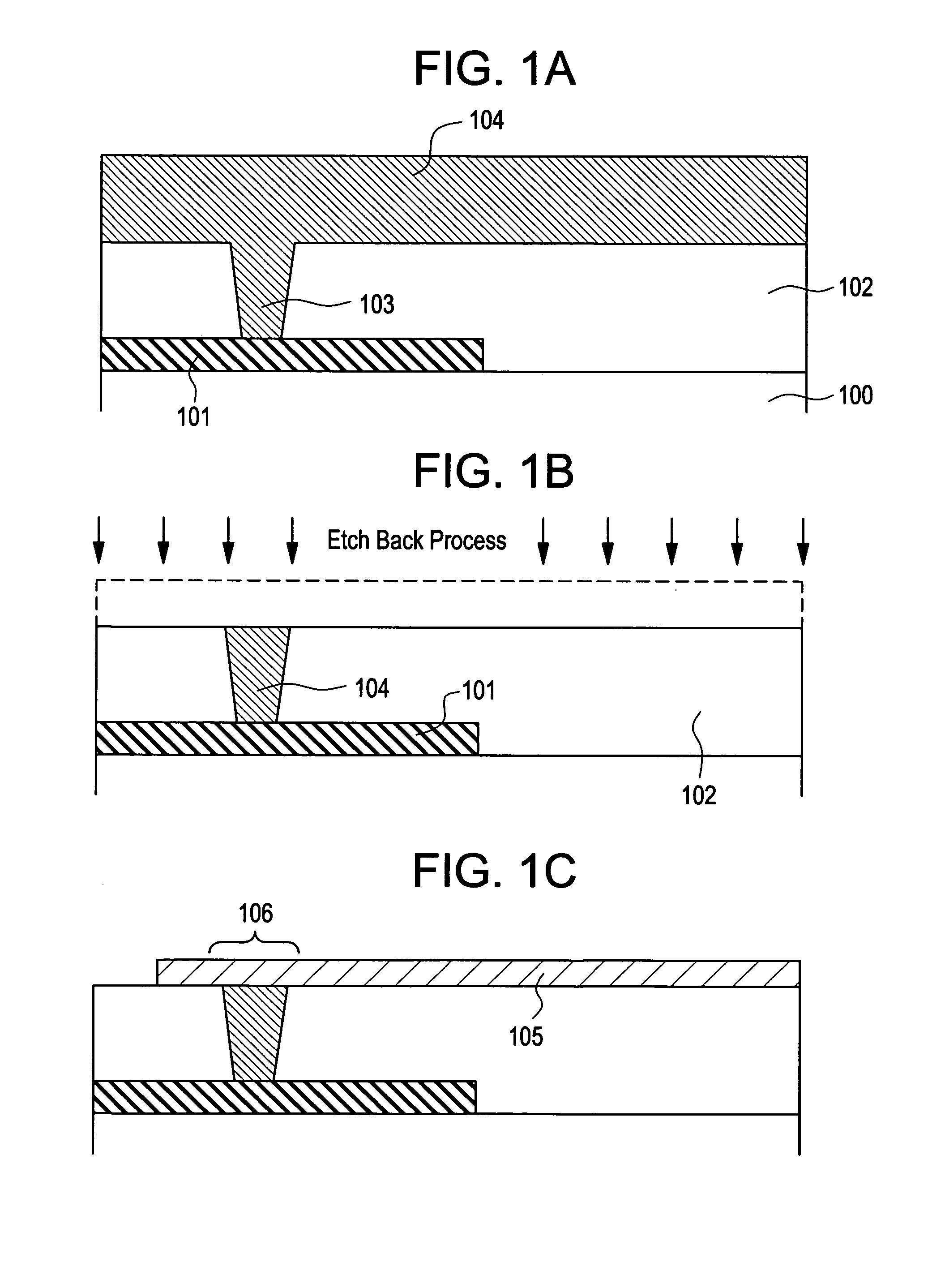
[0096]In this example, ITO is used as the embedded plug (conductive layer). In FIG. 2A, numeral 200 denotes an underlayer, which may be any of an insulating layer, a semiconductor layer or a conductive layer, and a first conductive layer 201 having a pattern is formed thereon.

[0097]The first conductive layer 201 is covered with an insulating layer (interlayer insulating layer) 202. As the insulating layer 202, an insulating film containing silicon such as silicon oxide, silicon nitride and silicon oxide-nitride, or an organic resin layer is used as a single layer or as having a multilayer structure.

[0098]After forming the insulating layer 202, an opening (contact hole) 203 is formed by etching. The method for etching may be a wet etching method or a dry etching method. It is effective that the cross sectional shape of the opening 203 is tapered to improve the coverage of a thin film subsequently formed.

[0099]After forming the opening 203, an oxide conductive layer 204 is formed. As ...

example 2

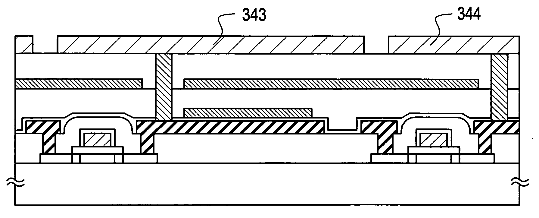
[0107]In this example, a production process of a unit pixel (unit picture element) constituting a pixel matrix circuit of an active matrix liquid crystal display device (AMLCD) driven in a reflection mode is described with reference to FIGS. 3A through 5C.

[0108]A quartz substrate 301 having an insulating surface is prepared. In this example, because a heat treatment at a temperature of from 900 to 1,1000° C. is conducted, a material having high heat resistance must be used. A crystalline glass (glass ceramics) substrate provided with an underlayer film and a silicon substrate provided with a thermal oxidized film may be used.

[0109]An amorphous silicon film 302 having a thickness of 65 nm is formed thereon, and the amorphous silicon film 302 is crystallized by using the technique described in Unexamined Published Japanese Patent Application No. 8-78329. The technique described in this publication is to conduct selective crystallization by using a catalytic element accelerating crysta...

example 3

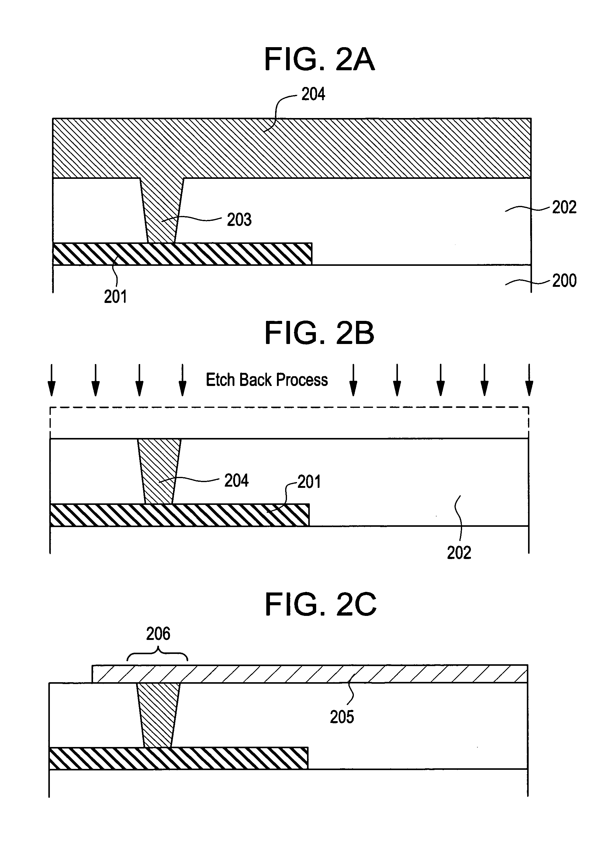
[0135]In this example, a production process of a unit pixel constituting a pixel matrix circuit of an active matrix liquid crystal display device (AMLCD) driven in a reflection mode using ITO as an embedded plug (conductive layer) is described with reference to FIGS. 6A through 8C.

[0136]A quartz substrate 601 having an insulating surface is prepared. In this example, because a heat treatment at a temperature of from 900 to 1,100° C. is conducted, a material having high heat resistance must be used. A crystalline glass (glass ceramics) substrate provided with an underlayer film and a silicon substrate provided with a thermal oxidized film may be used.

[0137]An amorphous silicon film 602 having a thickness of 65 nm is formed thereon, and the amorphous silicon film 602 is crystallized by using the technique described in Unexamined Published Japanese Patent Application No. 8-78329. The technique described in this publication is to conduct selective crystallization by using a catalytic el...


PUM

PropertyMeasurementUnit
diameteraaaaaaaaaa
diameteraaaaaaaaaa
diameteraaaaaaaaaa

Abstract

A semiconductor device and a process for producing the same, the semiconductor device comprising two conductive layers provided as separate layers, and an insulating layer sandwiched by the two conductive layers, in which the two conductive layers are electrically connected to each other with an embedded conductive layer or an oxide conductive layer provided as filling an opening formed in the insulating layer, and the embedded conductive layer comprises an organic resin film containing a conductive material dispersed therein or an inorganic film containing a conductive material dispersed therein.

Description

FIELD OF THE INVENTION[0001]The present invention relates to, in a semiconductor device using a thin film, a connection wiring ensuring electric connection between conductive thin films. Particularly, it relates to, in a pixel region of an active matrix liquid crystal display (AMLCD), a connection wiring ensuring electric connection between a switching element and a pixel electrode.[0002]The semiconductor device used herein involves all devices functioning by utilizing semiconductor properties, and an electro-optical device such as an AMLCD and a semiconductor circuit such as a microprocessor are included. Furthermore, an electronic apparatus containing such an electro-optical device and a semiconductor circuit is also included in the semiconductor device.BACKGROUND OF THE INVENTION[0003]Recently, the technique of providing a TFT on an inexpensive glass substrate is being rapidly developed. This is because the demand of an AMLCD is increased.[0004]In an AMLCD, each of several tens t...

Claims


Application Information

Patent Timeline
Patent Type & Authority Patents(United States)
IPC IPC(8): H01L29/04H01L31/036H01L31/0376H01L31/20G02F1/1362H01L21/77H01L21/84H01L27/12
CPCG02F1/1362H01L27/124G02F1/136227H01L21/76877
Inventor OHTANI, HISASHINAKAZAWA, MISAKOMURAKAMI, SATOSHI
Owner SEMICON ENERGY LAB CO LTD
Why Eureka
Try Eureka