
Field-effect semiconductor device

Inactive Publication Date: 2007-04-24
MURATA MFG CO LTD
View PDF8 Cites 7 Cited by
  • Summary
  • Abstract
  • Description
  • Claims
  • Application Information

AI Technical Summary

Benefits of technology

[0019]In order to solve the problems described above, an object of the present invention is to reduce series resistance through a semiconductor layer between a contact layer provided with an ohmic electrode and a channel layer in a field-effect semiconductor device having a heterojunction.
[0023]According to the present invention, since the resistance through the heterojunction portion between the channel layer and the semiconductor layer thereon can be reduced, and the resistance through the heterojunction portion between the contact layer and the semiconductor layer thereunder can also be reduced, a field-effect semiconductor device having low series resistance can be realized. In addition, since the Schottky barrier height in the thermal equilibrium can be reduced, phenomena such as applied-voltage-dependent increases and decreases in current (drain current kink) can be suppressed. Accordingly, a device can be produced having device characteristics in which the maximum drain current and mutual conductance are improved, and on-resistance is decreased.

Problems solved by technology

When the barrier height in the thermal equilibrium is high, the amount of increase and decrease in the barrier height is larger when the applied voltage is increased and decreased, and as a result, there is problems in that phenomena such as a drain current kink (see FIG. 6A) are generated, in which a drain current is abruptly increased at a certain voltage.

Method used


Image

  • Field-effect semiconductor device
  • Field-effect semiconductor device
  • Field-effect semiconductor device

Examples


first embodiment

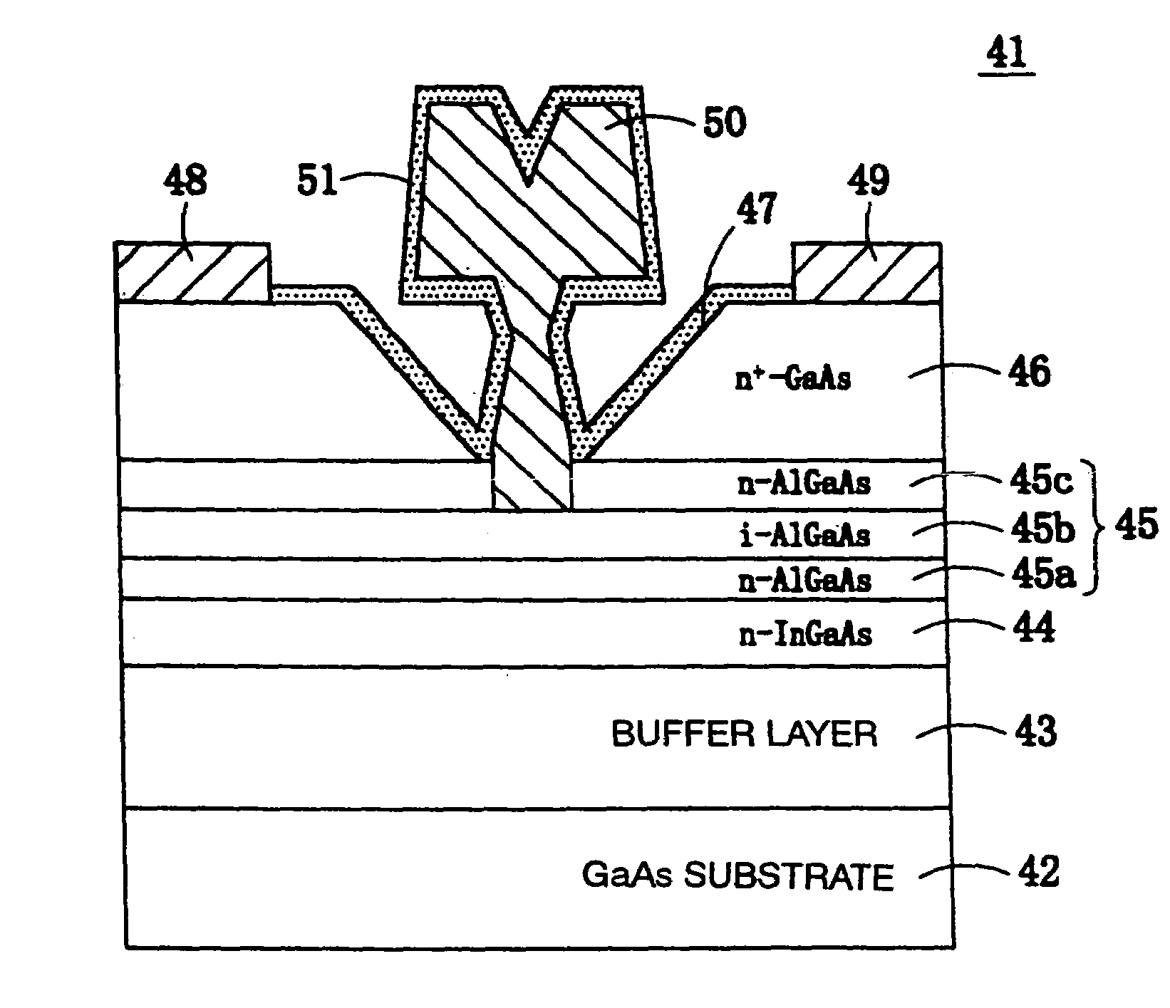
[0040]FIG. 4 is a schematic cross-sectional view of the structure of a heterojunction HEMT 41 according to an embodiment of the present invention. In the HEMT 41, a buffer layer 43, a channel layer 44 which is 10 nm thick composed of n-type InGaAs (the dopant concentration is 2×1018 cm−3), a barrier layer 45, and a contact layer 46 which is 50 nm thick composed of n+-type GaAs (the dopant concentration is 5×1018 cm−3) are formed in the order mentioned above on a semi-insulating GaAs substrate 42 by epitaxial growth using molecular beam epitaxy (MBE), metal-organic chemical vapor deposition (MOCVD), or the like. The barrier layer 45 is composed of, from the bottom thereof, an n-type AlGaAs layer 45a which is 10 nm thick (the dopant concentration is 3×1018 cm−3), an undoped AlGaAs film 45b which is 10 nm thick, and an n-type AlGaAs layer 54c which is 10 nm thick (the dopant concentration is 3×1018 cm−3).

[0041]Ohmic electrodes, which are used as a source electrode 48 and a drain electr...


PUM


Abstract

The field-effect semiconductor device includes a channel layer; a contact layer; a semiconductor structure having an electron-affinity different from those of the channel layer and the contact layer and formed between the channel layer and the contact layer; an ohmic electrode formed on the contact layer; and a Schottky electrode formed on the semiconductor structure. The junction face between the channel layer and the semiconductor structure and the junction face between the contact layer and the semiconductor structure are iso-type heterojunctions.

Description

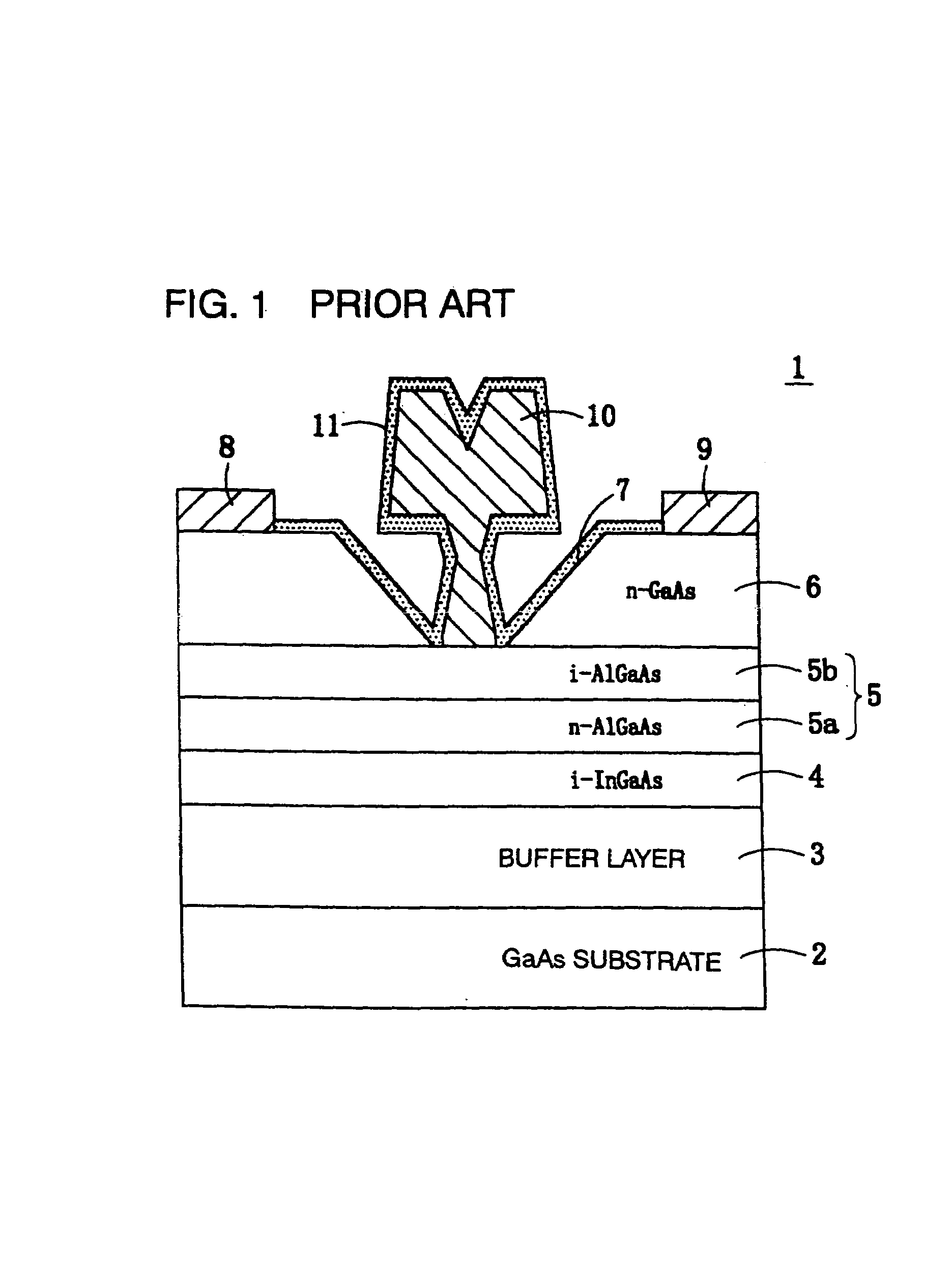
BACKGROUND OF THE INVENTION[0001]1. Field of the Invention[0002]The present invention relates to field-effect semiconductor devices, and more specifically, it relates to a field-effect semiconductor device having a heterojunction structure such as an HEMT structure or a DCHFET structure.[0003]2. Description of the Related Art[0004]Hitherto, as transistor devices operating in the region from microwaves to millimeter waves, a field-effect transistor having a heterojunction structure (hereinafter referred to as a heterojunction FET) has been used. In accordance with doped structures, the heterojunction FETs can be roughly classified into HEMTs (high-electron-mobility transistors) using a modulation-doped structure and DCHFETs (doped-channel heterojunction FETs) using a channel-doped structure. In this connection, the latter DCHFET is also called a DMT, an MISFET, an HIGFET, and the like.[0005]FIG. 1 is a schematic cross-sectional view showing a semiconductor structure of a conventional...

Claims


Application Information

Patent Timeline
IPC IPC(8): H01L31/00H01L29/812H01L21/338H01L29/778H01L29/80
CPCH01L29/802
Inventor INAI, MAKOTOSASAKI, HIDEHIKO
Owner MURATA MFG CO LTD
Learn More