Methods for forming single damascene via or trench cavities and for forming dual damascene via cavities

a damascene and cavity technology, applied in the direction of semiconductor devices, semiconductor/solid-state device details, electrical apparatus, etc., can solve the problems of etching deposited copper to form wiring patterns, insulation degradation and/or copper diffusion, via profile distortion, etc., to facilitate better via cd control, improve the selectivity of etch stop layer, and simplify the fabrication process flow

Inactive Publication Date: 2007-05-08
TEXAS INSTR INC
View PDF20 Cites 29 Cited by
  • Summary
  • Abstract
  • Description
  • Claims
  • Application Information

AI Technical Summary

Benefits of technology

[0009]The following presents a simplified summary in order to provide a basic understanding of one or more aspects of the invention. This summary is not an extensive overview of the invention, and is neither intended to identify key or critical elements of the invention, nor to delineate the scope thereof. Rather, the primary purpose of the summary is to present some concepts of the invention in a simplified form as a prelude to the more detailed description that is presented later. The invention relates to methods for fabricating single or dual damascene interconnect structures which may be employed to mitigate the above mentioned and other adverse effects. The invention may be employed to facilitate better via CD control, improve selectivity of etch-stop layer to IMD or ILD material, and / or to simplify the fabrication process flow.
[0011]In one implementation, the via etch and etch-stop etch are performed in-situ in a single etch tool, wherein the etch-stop etch is performed immediately after the via etch. The invention also provides for concurrent via and etch-stop etch operations, and for performing the etch-stop etch with at least a portion of the dielectric material covered. In one example, the etch-stop etch is performed immediately following the via etch, wherein the via etch resist remains covering the dielectric material during the etch-stop etch. Due to the presence of the resist during the etch-stop etch, more polymer deposition occurs on the via sidewalls to protect the via profile. In this manner, the invention may be employed so as to mitigate or avoid deleterious changes to the CDs and profiles of the resulting via or trench structures, and mitigates the reduction in dielectric thickness found in conventional processes. The invention facilitates simplification of the fabrication process flow to allow significant cost reduction, by eliminating the need for dedicated etch-stop etchers, freeing up ashers and wet hoods, and also allows significant reduction in cycle time. Moreover, the selectivity of etch-stop layer to IMD or ILD materials (e.g., SiC to OSG selectivity) may be improved, for example, due to the presence of resist during etch-stop etching.

Problems solved by technology

However, difficulties have been encountered in patterning (etching) deposited copper to form wiring patterns.
Furthermore, copper diffuses rapidly in certain types of insulation layers, such as silicon dioxide, leading to insulation degradation and / or copper diffusion through the insulation layers and into device regions.
Furthermore, the conventional via sidewalls become bowed during the etch-stop etch and intervening cleaning after the via etch process, leading to via profile distortion.

Method used


Image

  • Methods for forming single damascene via or trench cavities and for forming dual damascene via cavities
  • Methods for forming single damascene via or trench cavities and for forming dual damascene via cavities
  • Methods for forming single damascene via or trench cavities and for forming dual damascene via cavities

Examples


Embodiment Construction

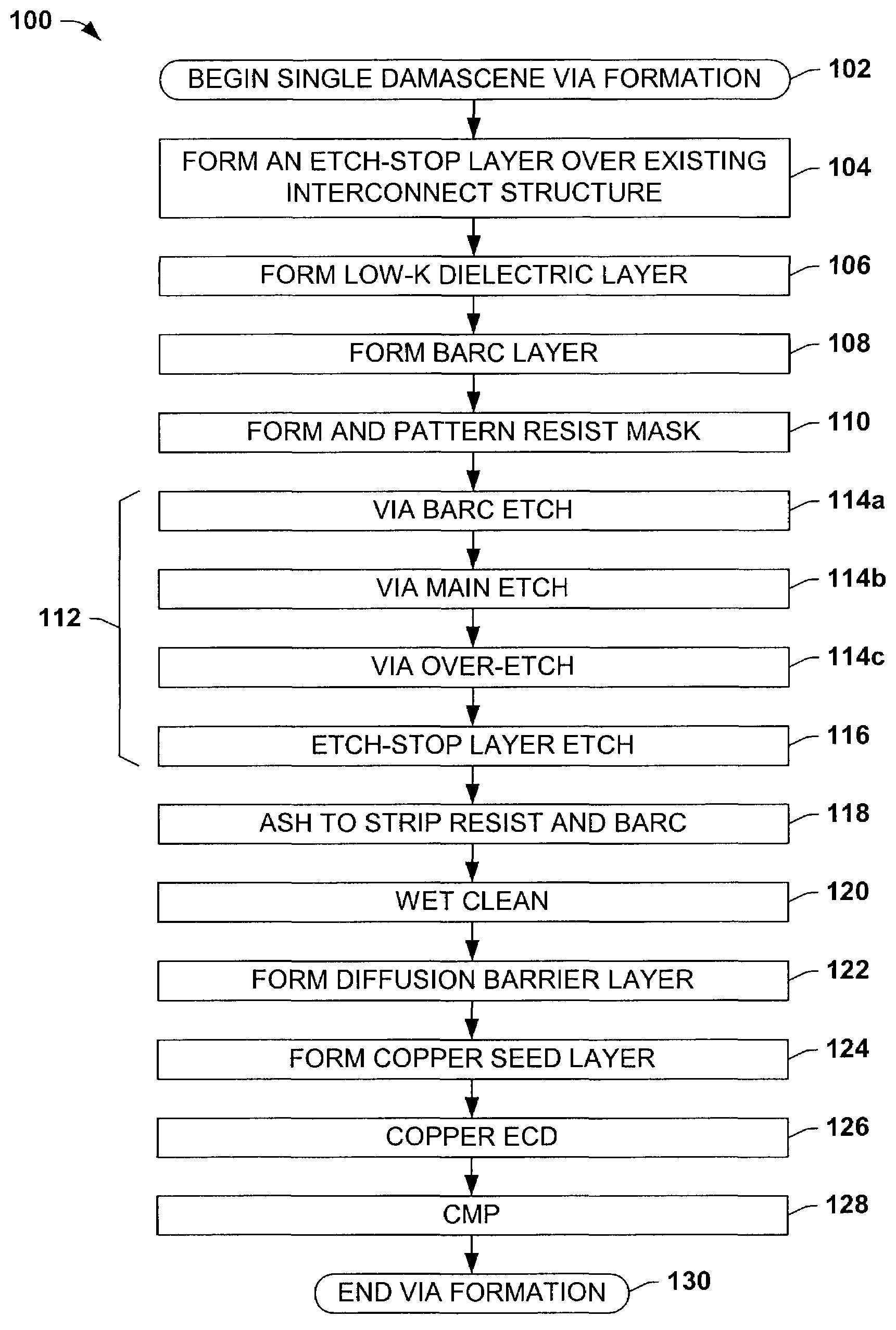
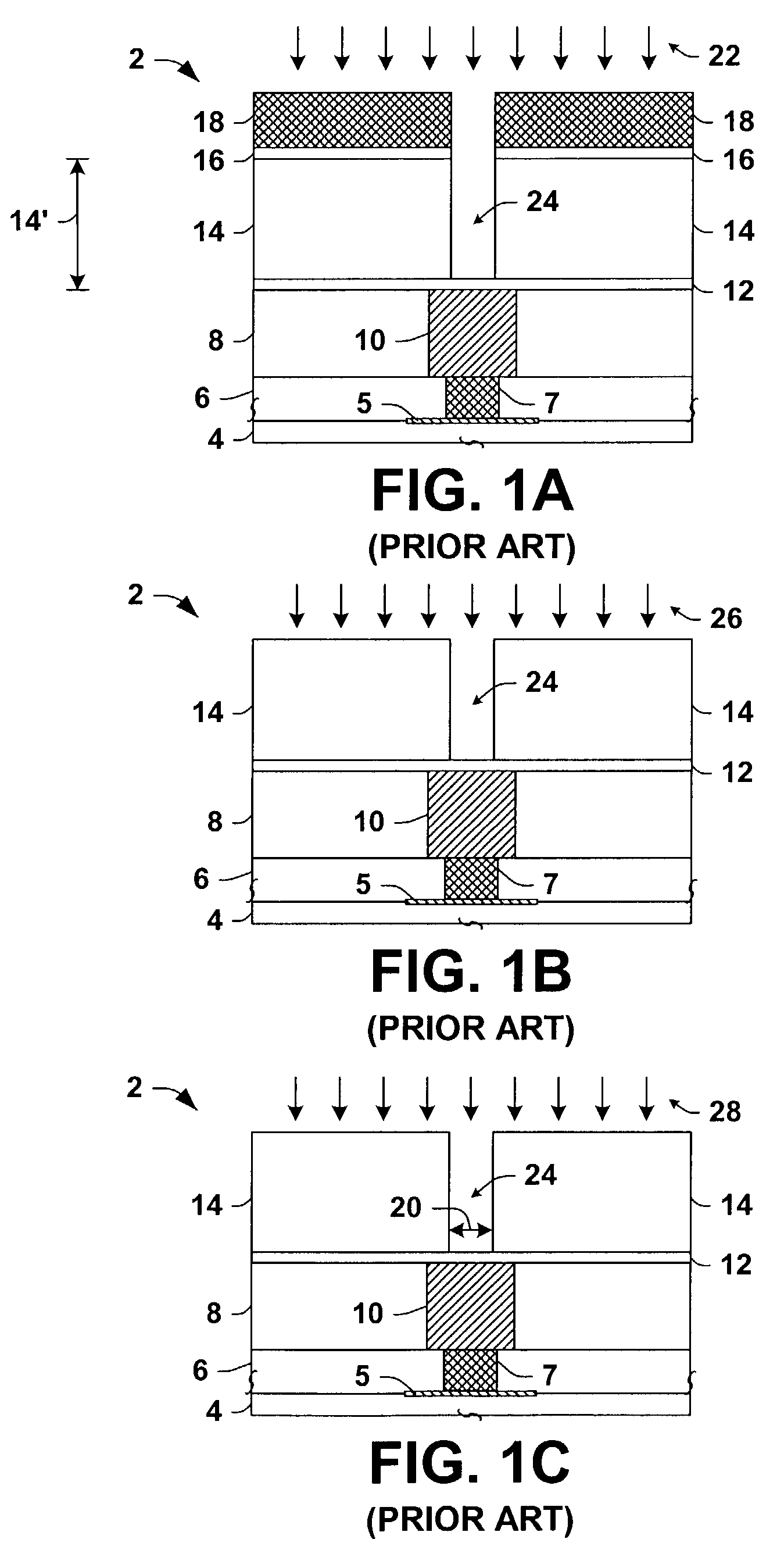
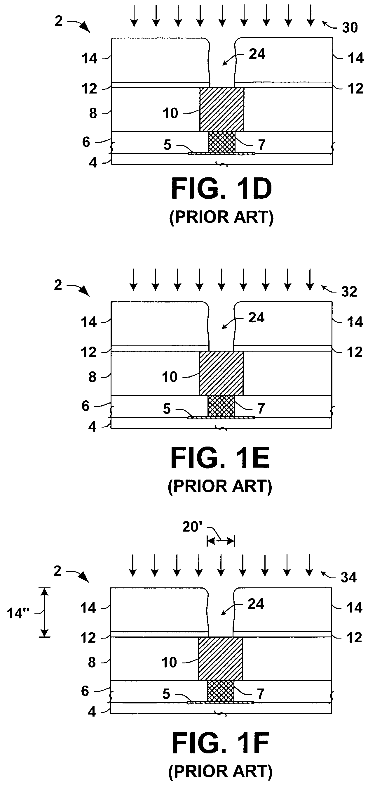
[0026]The present invention will now be described with reference to the attached drawings, wherein like reference numerals are used to refer to like elements throughout. The invention relates to methods for forming single and / or dual damascene interconnect structures, including via and / or trench cavities or openings during interconnect processing of integrated circuits and other semiconductor devices. One or more implementations of the invention are hereinafter illustrated and described in the context of single or dual damascene trench and / or via cavity formation in low-k organo-silicate-glass (OSG) structures, where silicon carbide (SiC) etch-stop layers are employed. However, it will be appreciated by those skilled in the art that the invention is not limited to the exemplary implementations illustrated and described hereinafter. In particular, the various aspects of the invention may be employed in association with processing of devices using OSG, FSG, or other low-k or ultra low...


PUM


Abstract

Methods are disclosed for forming trench or via cavities in a single damascene interconnect structure, comprising etching a dielectric layer to form a cavity there and to expose an underlying etch-stop layer, and etching the exposed etch-stop layer to extend the cavity and to expose a conductive feature in an existing interconnect structure, wherein etching the portion of the dielectric layer and etching the exposed portion of the etch-stop layer are performed concurrently with substantially no intervening processing steps therebetween. Also disclosed are methods of forming a via cavity in a dual damascene interconnect structure, comprising forming an etch-stop layer over an existing interconnect structure, forming a dielectric layer over the etch-stop layer, etching a portion of the dielectric layer to form a via cavity in the dielectric layer and to expose a portion of the etch-stop layer, and etching the etch-stop layer to extend the via cavity, where the dielectric layer is covered during etching of the etch-stop layer.

Description

FIELD OF INVENTION[0001]The present invention relates generally to semiconductor devices and more particularly to methods for fabricating single and dual damascene interconnect structures in the fabrication of semiconductor devices.BACKGROUND OF THE INVENTION[0002]In the manufacture of semiconductor products such as integrated circuits, individual electrical devices are formed on or in a semiconductor substrate, and are thereafter interconnected to form electrical circuits. Interconnection of these devices within an integrated circuit is typically accomplished by forming a multi-level interconnect network structure in layers formed over the electrical devices, by which the device active elements are connected to other devices to create the desired circuits. Individual wiring layers within the multi-level network are formed by depositing an insulating or dielectric layer over the discrete devices or over a previous interconnect layer, and patterning and etching contact openings such ...

Claims


Application Information

Patent Timeline
Patent Type & Authority Patents(United States)
IPC IPC(8): H01L21/44H01L21/4763H01L21/3065H01L21/768H01L23/522
CPCH01L21/76802H01L21/76808
Inventor JIANG, PINGKRAFT, ROBXING, GUOQIANGKIRMSE, KAREN H. R.ZIELINSKI, EDEN
Owner TEXAS INSTR INC
Why Eureka
Try Eureka