Power and ground shield mesh to remove both capacitive and inductive signal coupling effects of routing in integrated circuit device

Inactive Publication Date: 2007-05-15
SYNOPSYS INC
View PDF6 Cites 24 Cited by
  • Summary
  • Abstract
  • Description
  • Claims
  • Application Information

AI Technical Summary

Problems solved by technology

As Very Deep Sub-Micron (VDSM) technologies continue to reduce in size (for example from 0.18 uM, 0.15 uM, 0.13 uM, 0.11 uM and beyon

Method used


Image

  • Power and ground shield mesh to remove both capacitive and inductive signal coupling effects of routing in integrated circuit device
  • Power and ground shield mesh to remove both capacitive and inductive signal coupling effects of routing in integrated circuit device
  • Power and ground shield mesh to remove both capacitive and inductive signal coupling effects of routing in integrated circuit device

Examples


embodiment 400

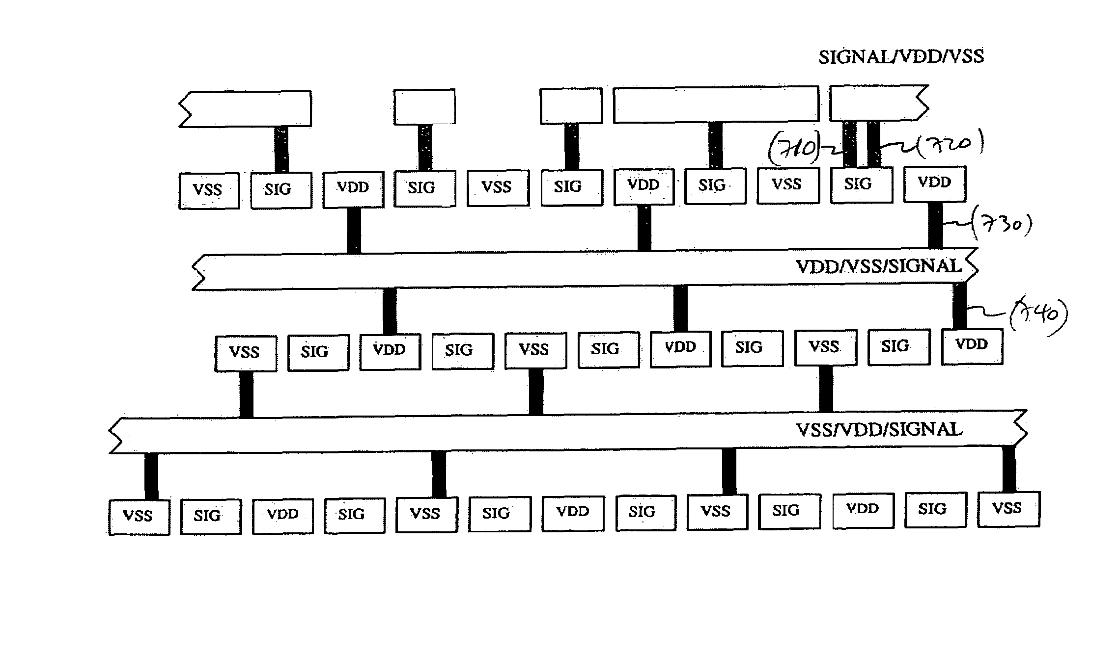
[0034]FIG. 4 is a top view of shield mesh embodiment 400 showing two adjacent substrate layers, 405A and 405B, depicting the signal lines (410, 420 and 430), alternating VDD and VSS lines on each layer and the appropriate vias between the two layers utilizing a grid layout. Each via provides layer connections and also reduces the segment size of the shielding mesh and thereby reduces the effective R-C resistance according to one embodiment of the present invention. It is important to note that on layer N, 405A, if the signal lines 410, 420 and 430 are on odd grid tracks, then the VDD and VSS lines will be on even grid tracks, and vice-versa. Like wise, on layer N+1, 405B, if the signal lines 440, 450 and 460 are on even tracks, then the VDD and VSS lines will alternately be on odd grid tracks and vice-versa.

[0035]Multi-layer routing assignment to signals and shields: for the vertical space, the track assignment should be done so that there would not be signal tracks directly on top ...

embodiment 900

[0040]FIG. 9 depicts embodiment 900, which depicts a shielding mesh in the routing channel (910) between blocks on a substrate and also within a block (920) of a substrate. As described in FIG. 8, due to relative small segment lengths of the shielding mesh, the shielding mesh further reduces the effective RC component of the routing line thereby reducing the noise and coupling effects caused by cross-talk between signal lines.

[0041]FIG. 10 illustrates the flow chart of steps for the process, 1000, of an EDA tool in which the shielding mesh of the present invention may be introduced. As shown in this embodiment of the present invention, initial code is generally written using HDL, step 1010, (for example) after which logic synthesis, step 1020, is performed. Placement of a power grid is next performed as shown in block 1030. For example where substrate grid is utilized, shielding mesh as outlined in one embodiment of the present invention can be introduced as shown at point 1040. Aft...


PUM


Abstract

A power and ground shield mesh to remove both capacitive and inductive signal coupling effects of routing in integrated circuit device. An embodiment describes the routing of a shield mesh of both power and ground lines to remove noise created by capacitive and inductive coupling. Relatively long signal lines are routed in between fully connected power and ground shield mesh which may be generated by a router during the signal routing phase or during power mesh routing phase. Leaving only the odd tracks or the even tracks for signal routing, power mesh (VDD) and ground mesh (VSS) are routed and fully interconnected leaving shorter segments and thereby reducing the RC effect of the circuit device. Another embodiment presents a technique where the signals are shielded using the power and ground mesh for a gridless routing. Another embodiment presents a multi-layer grid routing technique where signals are routed on even grid and the power and ground lines are routed on odd grid. A similar embodiment represents grid routing technique where the signals are routed between layers N and N+1. Another embodiment enables signals to be shielded by opposite power and ground grids on left, right, top and bottom. Additional embodiments also include utilization of similar mesh utilized in standard cell and/or in the gate array routing area or any other area where any other signal line is to be shielded.

Description

[0001]This application is a continuation application of U.S. patent application Ser. No. 10 / 132,996, filed on Apr. 25, 2002 now U.S. Pat. No. 6,734,472.BACKGROUND OF THE INVENTION[0002]1. Field of the Invention[0003]The field of the present invention pertains to circuitry to solve the problems caused by capacitive and inductive coupling in signals in an integrated circuit device. This particular issue of capacitive and inductive coupling in signals is becoming increasingly difficult as the industry advances and moves towards reduction in circuit device size (for example, from 0.25 uM technology to 0.18 uM, 0.15 uM, 0.13 uM and beyond).[0004]2. Related Art[0005]With their growth in commercial markets and consumer demands for smaller Integrated Circuits (ICs—which are used in numerous applications such as cellular phones, wristwatch cameras, and hand-held organizers just to name a few) increase, IC size requirement trends continue towards a small form factor and lowered power consumpt...

Claims


Application Information

Patent Timeline
IPC IPC(8): H05K1/00H05K9/00H01L21/82H01L21/822H01L23/522H01L27/04H01L27/118
CPCH01L23/5225H01L23/5286H01L27/118H01L2924/3011H01L2924/0002H01L2924/00
Inventor HO, IU-MENG TOM
Owner SYNOPSYS INC
Why Eureka
Try Eureka