
Semiconductor device

Active Publication Date: 2007-05-15
SEMICON ENERGY LAB CO LTD
View PDF60 Cites 40 Cited by
  • Summary
  • Abstract
  • Description
  • Claims
  • Application Information

AI Technical Summary

Benefits of technology

[0029]The present invention has been devised in view of the above problems. Therefore, an object of the invention is to provide a semiconductor device in which the number of manufacturing steps is reduced by using transistors having a single polarity (i.e. having the same conductivity type) to constitute each pixel, thereby achieving increased yield and reduced costs. Another object of the present invention is to provide a semiconductor device in which a photoelectric conversion element can attain a sufficient signal amplitude.
[0030]In order to attain the above objects, according to the present invention, there is provided a semiconductor device in which each pixel is provided with an electric circuit (a bootstrap circuit) for generating an electric potential that is higher than a voltage given through capacitative coupling. Further, according to the present invention, there is provided a semiconductor device in which a sufficient signal amplitude can be attained by using the above electric circuit to set a potential difference between both terminals of a photoelectric conversion element to the same value as the power source potential. Still further, according to the present invention, there is provided a semiconductor device in which the number of manufacturing steps are reduced by using transistors having a single polarity to constitute each pixel, to thereby achieve increased yield and reduced costs.
[0032]According to the present invention configured as described above, it is possible to provide a semiconductor device in which the number of manufacturing steps is reduced by using transistors having a single polarity (i.e. having the same conductivity type), thereby achieving increased yield and reduced costs. Also, according to the present invention, it is possible to provide a semiconductor device in which a photoelectric conversion element thereof can attain a sufficient signal amplitude, whereby the photoelectric conversion element can read out a subject with higher precision.

Problems solved by technology

In such a case, it becomes difficult to read information of a subject with precision.
The resulting complexity of its manufacture has been the source of reduced yield and increased manufacturing costs.
However, amplitude attenuation occurs in the above-mentioned pixels, thus making it impossible to attain a sufficient signal amplitude.
However, the pixel 100 includes transistors having mutually different conductivity types, which adds complexity to its manufacture.

Method used


Image

  • Semiconductor device
  • Semiconductor device
  • Semiconductor device

Examples


embodiment 1

[Embodiment 1]

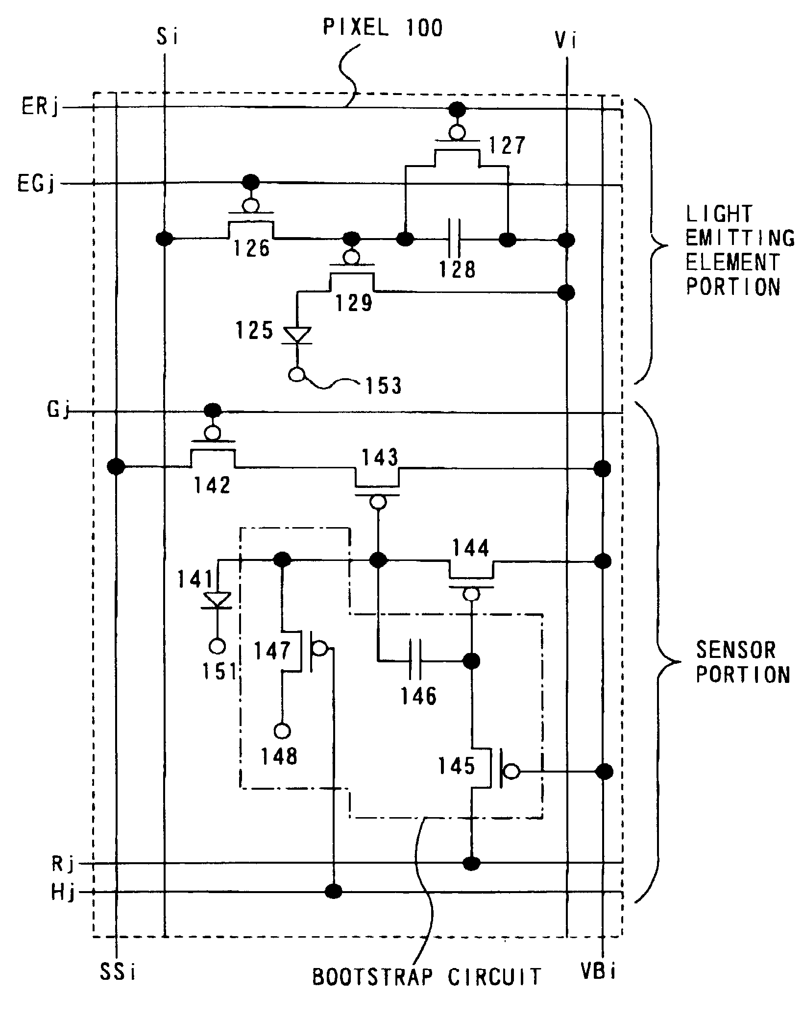
[0090]In Embodiment 1, description will be made with respect to a case where the present invention is applied to a semiconductor device in which a light emitting element and a photoelectric conversion element are provided in each pixel, with reference to FIGS. 7 to 8.

[0091]FIG. 7 is a schematic diagram showing a semiconductor device of the present invention. The semiconductor device shown in FIG. 7 includes a pixel portion 130 and a plurality of driver circuits arranged in the periphery of the pixel portion 130. The pixel portion 130 is roughly divided into a light-emitting-element portion and a sensor portion. The plurality of driver circuits include: a source signal line driver circuit 131, a gate signal line driver circuit 132, and a reset signal line driver circuit 133 which perform control of the light-emitting-element portion; and a source signal line driver circuit 134 for sensor, a gate signal line driver circuit 135 for sensor, a reset signal line driver circu...

embodiment 2

[Embodiment 2]

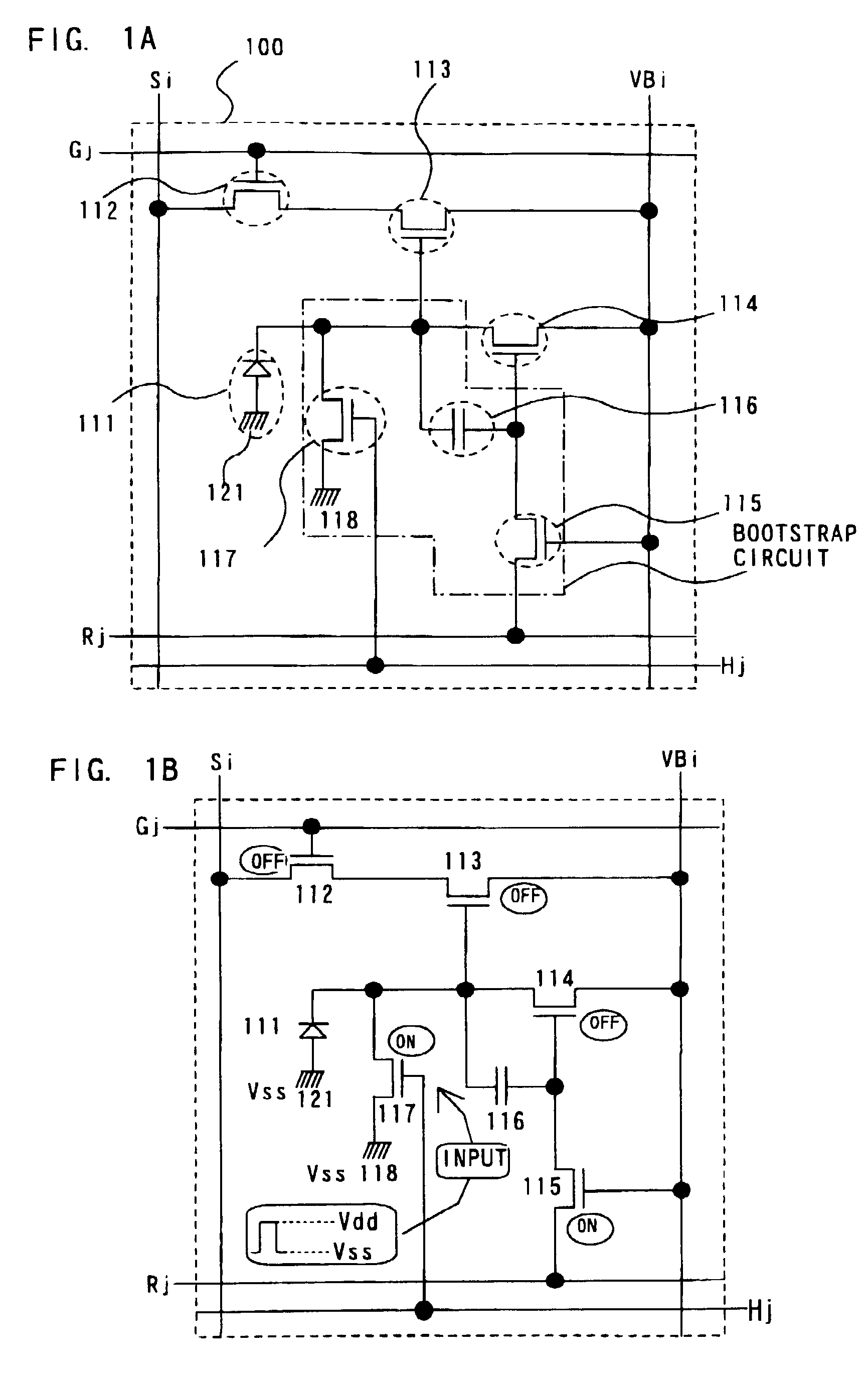
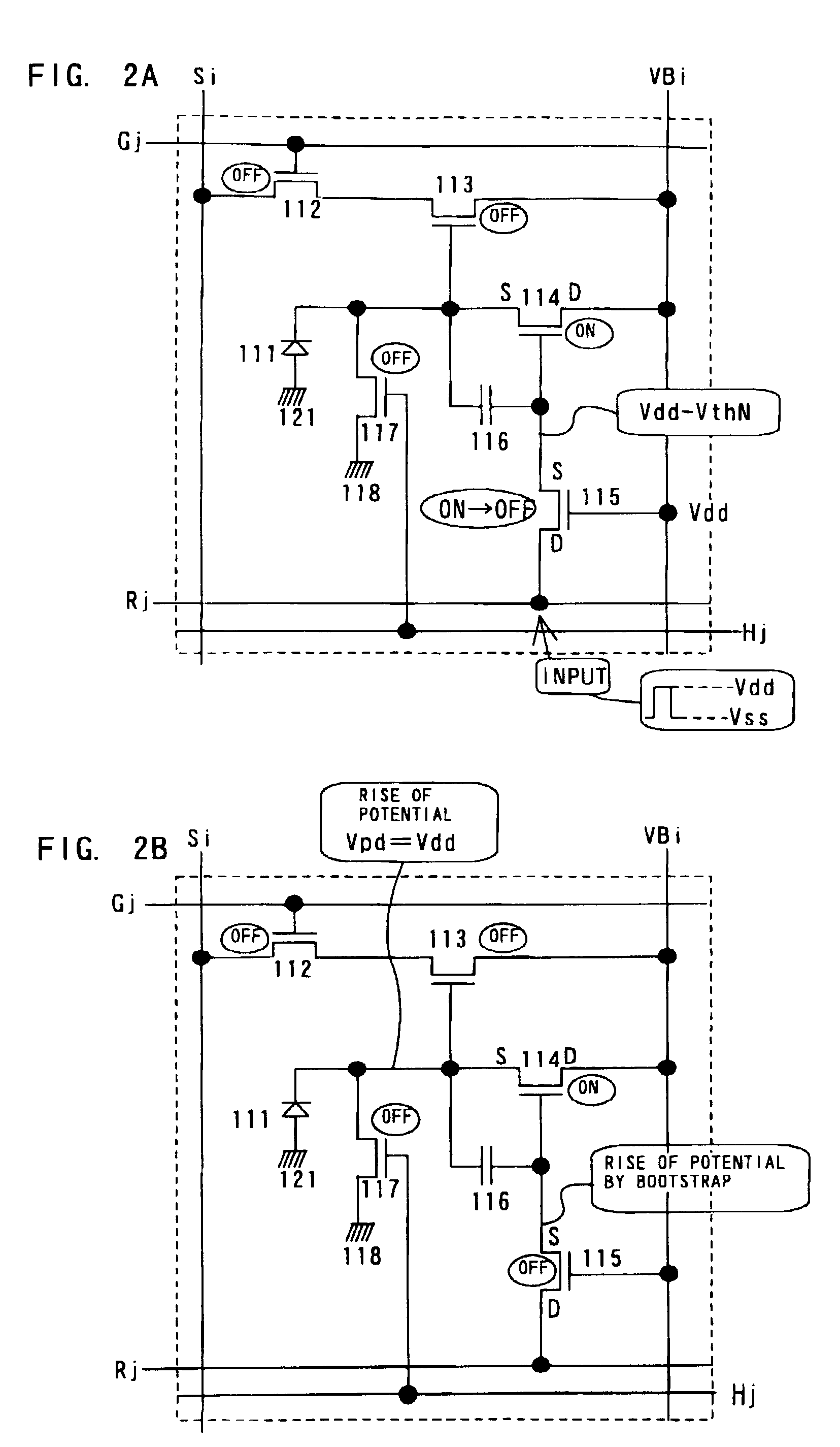
[0114]This embodiment gives a description of methods of manufacturing a pixel portion in which photoelectric conversion elements and transistors are provided on the same insulator surface and a driver circuit formed in the periphery of the pixel portion by single polarity transistor with references to FIGS. 5 and 6.

[0115]First, as shown in FIG. 5A, a base film 5002 is formed from an insulating film such as a silicon oxide film, a silicon nitride film, and a silicon oxynitride film on a glass substrate 5001. The substrate 5001 is formed of barium borosilicate glass typical example of which is Corning #7059 glass or Corning #1737 glass (product of Corning Incorporated), or of aluminoborosilicate glass. The base film 5002 is, for example, (not shown) a laminate of a silicon oxynitride film that is formed from SiH4, NH3, and N2O by plasma CVD to a thickness of 10 to 200 nm (preferably 50 to 100 nm) and a silicon oxynitride hydride film formed from SiH4 and N2O by plasma CV...

embodiment 3

[Embodiment 3]

[0149]In this embodiment, a manufacturing steps of the pixel portion in which the photoelectric conversion element, the light emitting element, and transistor are provided on the same insulating surface, and the driver circuit in the periphery of the pixel portion by using a single polarity transistor are described with references to FIGS. 9A to 10B.

[0150]As above mentioned in Embodiment 2, the manufacturing method of the pixel portion and driver circuit of the periphery thereof formed by only n-channel type transistors are described. In the n-channel type transistor, the impurity region referred to as an overlap region is provided at the region overlapped with the gate electrode to restrain the hot carrier deterioration. On the contrary, in the p-channel type transistor, the overlap region is not necessary to be formed, because the influence of the p-channel type transistor due to the hot career deterioration is small. The p-channel type transistor can be formed by mo...


PUM


Abstract

A semiconductor device is provided in which each pixel includes an electric circuit (a bootstrap circuit) for generating an electric potential that is higher than a voltage given through capacitative coupling. Also, there is provided a semiconductor device in which a sufficient signal amplitude can be attained by using the electric circuit to set a potential difference between both terminals of a photoelectric conversion element to the same value as the power source potential. Further, there is provided a semiconductor device in which the number of manufacturing steps is reduced by using transistors having a single polarity to constitute each pixel, thereby achieving increased yield and reduced costs.

Description

BACKGROUND OF THE INVENTION[0001]1. Field of the Invention[0002]The present invention relates to a semiconductor device having an image sensor function.[0003]2. Description of the Related Art[0004]A semiconductor device having an image sensor function is generally provided with a photoelectric conversion element and one or plural transistors for controlling the photoelectric conversion element.[0005]There are roughly two types of semiconductor devices having an image sensor function: CCD type semiconductor devices and CMOS type semiconductor devices. The CMOS type semiconductor devices are subdivided into those of a passive type with no amplification circuit mounted therein and those of an active type with an amplification circuit mounted therein. An amplification circuit has a function of amplifying an image signal of a subject read by a photoelectric conversion element, making the obtained signal less susceptible to an influence of noise. Accordingly, active CMOS type semiconducto...

Claims


Application Information

Patent Timeline
IPC IPC(8): H04N3/14H01L27/146H01L27/15
CPCH01L27/14665
Inventor KIMURA, HAJIME
Owner SEMICON ENERGY LAB CO LTD
Features
  • Generate Ideas
  • Intellectual Property
  • Life Sciences
  • Materials
  • Tech Scout
  • Unparalleled Data Quality
  • Higher Quality Content
  • 60% Fewer Hallucinations
Learn More