System and method for detecting defects in semiconductor wafers

a technology of semiconductor wafers and defect delineation, which is applied in the direction of optics, optical radiation measurement, instruments, etc., can solve the problems of incomplete manufacturing process, defects still created in wafers, and full area of wafers, and achieves non-destructive, cheap, and rapid

Active Publication Date: 2007-05-22
THE UNIV OF NORTH CAROLINA AT CHAPEL HILL
View PDF5 Cites 16 Cited by
  • Summary
  • Abstract
  • Description
  • Claims
  • Application Information

AI Technical Summary

Benefits of technology

[0011]The above objectives are achieved according to this invention by utilizing a polarized light microscope for performing a rapid, inexpensive, and non-destructive defect delineation of defects including micropipes, stressed striations, inclusions, dislocations, and grain boundaries. This invention can easily determine the location and therefore map defects of wafers including expitoxial films such as SiC, GaN, AlN and AlGaN. The invention provides for A system for delineating defects in a semiconductor wafer comprising a computer readable medium in communications with a CCD and a display monitor, an analyzer disposed adjacent to the CCD for analyzing polarized light received by the CCD and transmitted through the semiconductor wafer, a polarized light source for transmitting light through the semiconductor wafer so that the CCD can receive image information representing defects illuminated by the polarized light; and, a set of computer readable instructions included within the computer readable medium for allocating a plurality of scan regions associated with the semiconductor wafer, receiving scan information representing at least one scan region from the CCD, and displaying the scan information on the display monitor so that defects of the semiconductor wafer illuminated by the polarized light may be rapidly determined in a non-destructive manner. The system can also contain computer readable instructions for storing the scan information within the computer readable medium, cumulating the scan information to create a digital map representing the entire area of the semiconductor wafer and displaying the digital map. A movable scanning plate can be included, having an actuator, in communications with the computer readable medium; and, the set of computer readable instructions include instructions for receiving wafer placement information representing the location of th

Problems solved by technology

However, the manufacturing process is not perfect and wafers are still created that contain defects.
Some of these defects prevent the full area of the wafer from being used as any device located over such a defect causes the device to fail or otherwise become inoperable.
Unfortunately, SiC wafers contain defects, including dislocations such as threading edge, screw, and basal plane dislocations, and stacking faults.
The existence of micropipes and screw dislocations in the wafer, especially in high densities, prevents the use of large device areas for more powerful and complex devices.
In fact, micropipes and screw dislocations have been identified as the main obstacle for commercializing large-area power devices.
Micropipes lead to premature reverse breakdown in the SiC p-n junction and clearly adversely affect the electrical performance of the SiC device.
However, both are destructive methods resulting in a non-usable SiC wafer and not well suited for production line testing.
While other methods exist, they require expensive equipment or special facilities.
Other methods, such as atomic force microscopy (AFM), sc

Method used


Image

  • System and method for detecting defects in semiconductor wafers
  • System and method for detecting defects in semiconductor wafers
  • System and method for detecting defects in semiconductor wafers

Examples


Embodiment Construction

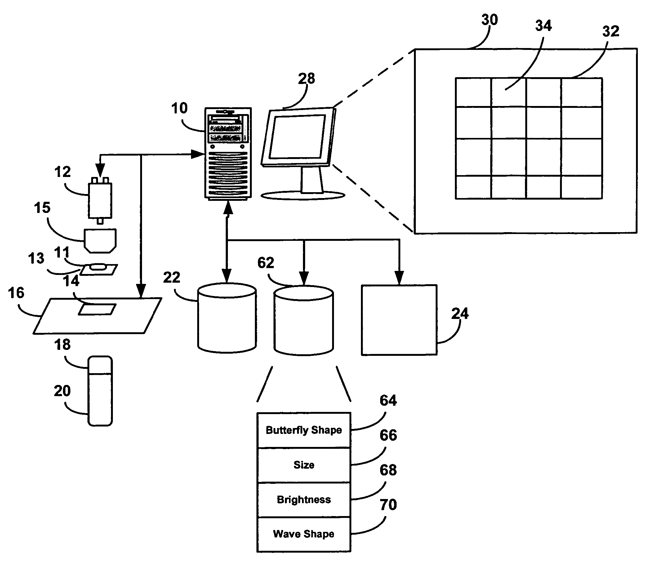
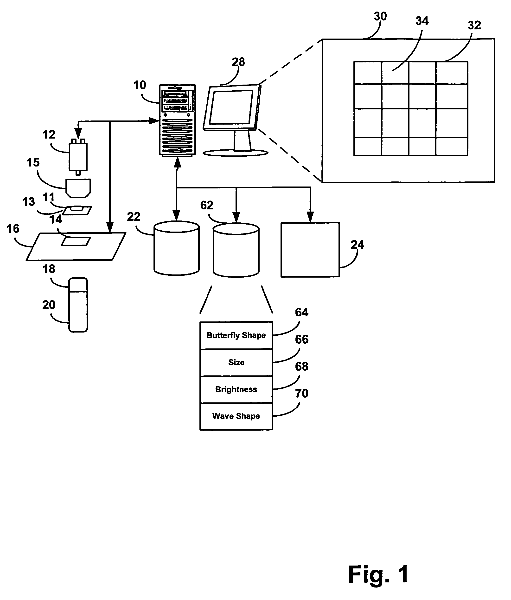
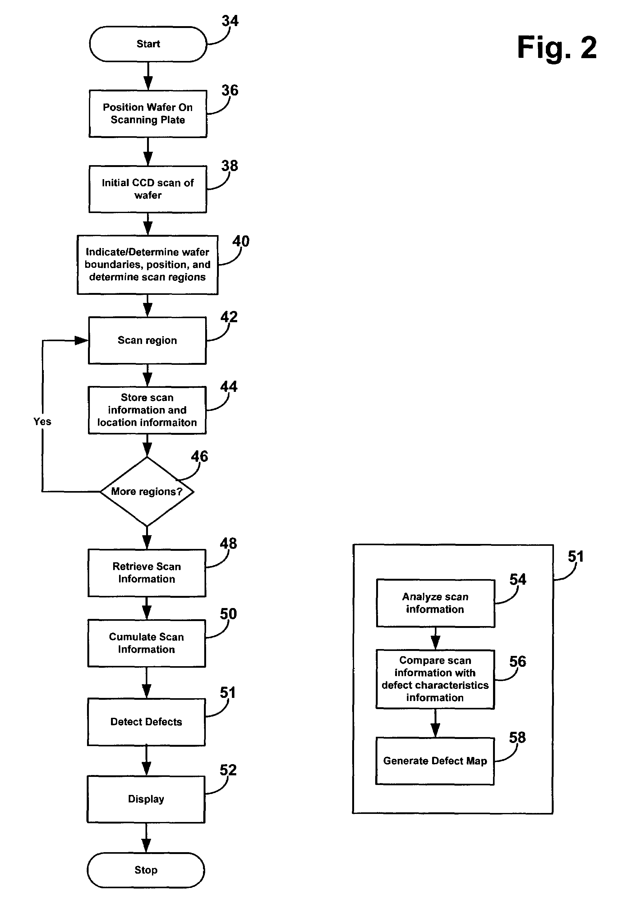
[0016]The detailed description that follows may be presented in terms of program procedures executed on a computer or network of computers. These procedural descriptions are representations used by those skilled in the art to most effectively convey the substance of their work to others skilled in the art. These procedures herein described are generally a self-consistent sequence of steps leading to a desired result. These steps require physical manipulations of physical quantities such as electrical or magnetic signals capable of being stored, transferred, combined, compared, or otherwise manipulated computer readable medium that is designed to perform a specific task or tasks. Actual computer or executable code or computer readable code may not be contained within one file or one storage medium but may span several computers or storage mediums. The term “host” and “server” may be hardware, software, or combination of hardware and software that provides the functionality described ...


PUM


Abstract

A system and method for detecting defects in semiconductor wafers in a rapid non-destructive manner. Defects in semiconductor wafers can include micropipes and screw dislocations, stress striations, planer defects, polytype inclusions, and others. When a wafer is illuminated by polarized light, the defects induce birefringence of the polarized light that can be visualized by a polariscope to detect defects in wafers. Defects can cause linearly inputted polarized light to emerge as elliptically polarized light after transmission through a wafer having defects. Placing the wafer between a set of polarizers under the cross poles condition allows for a rapid non-destructive system and method for delineating and locating defects within a semiconductor wafer.

Description

FIELD OF THE INVENTION [0001]This invention is directed to a system and method for determining defect delineation in semiconductor wafers and more specifically a non-destructive system and method for utilizing polarized light microscopy to delineate and map defects in semiconductor wafers.BACKGROUND OF THE INVENTION [0002]Semiconductor devices, such as diodes, transistors, and integrated circuits are found everywhere in modern society. These devices are used in automobiles, cell phones, computers, televisions, satellites, and many other products. The semiconductor market has grown at a staggering pace over the years with improvements in performance and reduction in cost measured in orders of magnitude. This drastic improvement in semiconductor technology is due to the skill and technology advances in the ability to miniaturize devices so that more complicated devices can occupy smaller footprints on a wafer. The technology for the manufacture of semiconductors, specifically silicon ...

Claims


Application Information

Patent Timeline
IPC IPC(8): G01N21/88G01J4/00G01N21/00G01N21/86G02F1/01G01N21/95
CPCG01N21/21G01N21/8851G01N21/9501
Inventor MA, XIANYUNSUDARSHAN, TANGALI S.
Owner THE UNIV OF NORTH CAROLINA AT CHAPEL HILL
Why Eureka
Try Eureka