Semiconductor device with mushroom electrode and manufacture method thereof

Inactive Publication Date: 2007-05-29
FUJITSU LTD +1
View PDF14 Cites 2 Cited by
  • Summary
  • Abstract
  • Description
  • Claims
  • Application Information

AI Technical Summary

Benefits of technology

[0013]It is an object of the present invention to provide a semiconductor device having a fine gate capable of being manufactured with a high yield.
[0022]As above, a semiconductor device having mushroom gate electrodes can be manufactured highly reliably. Even if the gate length is short, a mushroom gate electrode can be formed with a high yield.

Problems solved by technology

As the aspect ratio of a vertical opening to be formed in a resist layer becomes large, it becomes difficult to uniformly bury the lower vertical opening with a gate electrode layer.
A conventional tapering method is, however, insufficient in that a uniform opening shape and a gate electrode cross-sectional shape at the contact area between semiconductor and the gate electrode cannot be formed reliably.
This conventional method has, however, poor controllability so that a uniform gate length is difficult to be set.
Because of poor controllability, the cross section at the contact between semiconductor and the gate electrode is difficult to be controlled and an operation speed and reliability of devices cannot be improved.
This method has, however, poor controllability and is difficult to obtain a uniform opening length, i.e., gate length.
Because of poor controllability, it is difficult to control the cross section of the contact area between semiconductor and the gate electrode and improve the operation speed and reliability of devices.

Method used


Image

  • Semiconductor device with mushroom electrode and manufacture method thereof
  • Semiconductor device with mushroom electrode and manufacture method thereof
  • Semiconductor device with mushroom electrode and manufacture method thereof

Examples


Embodiment Construction

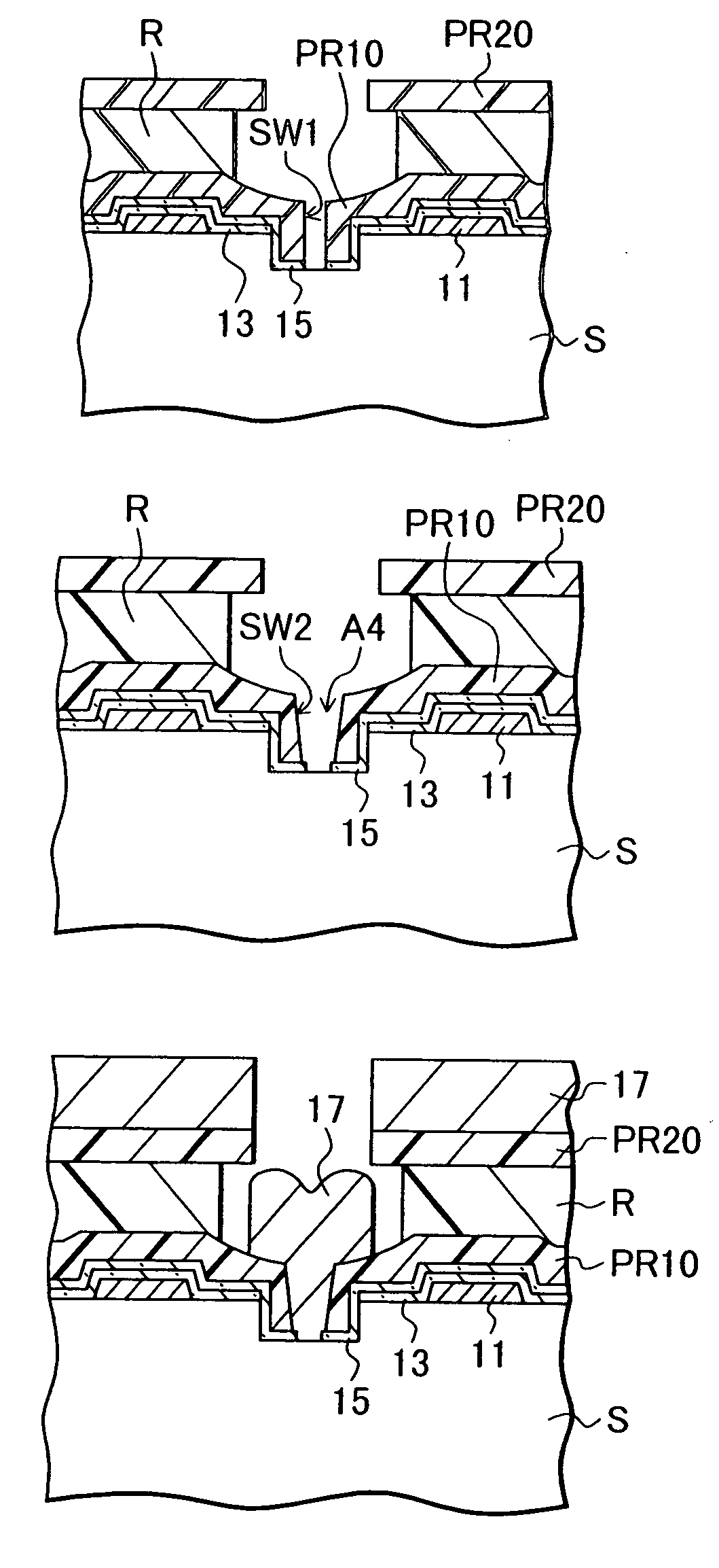
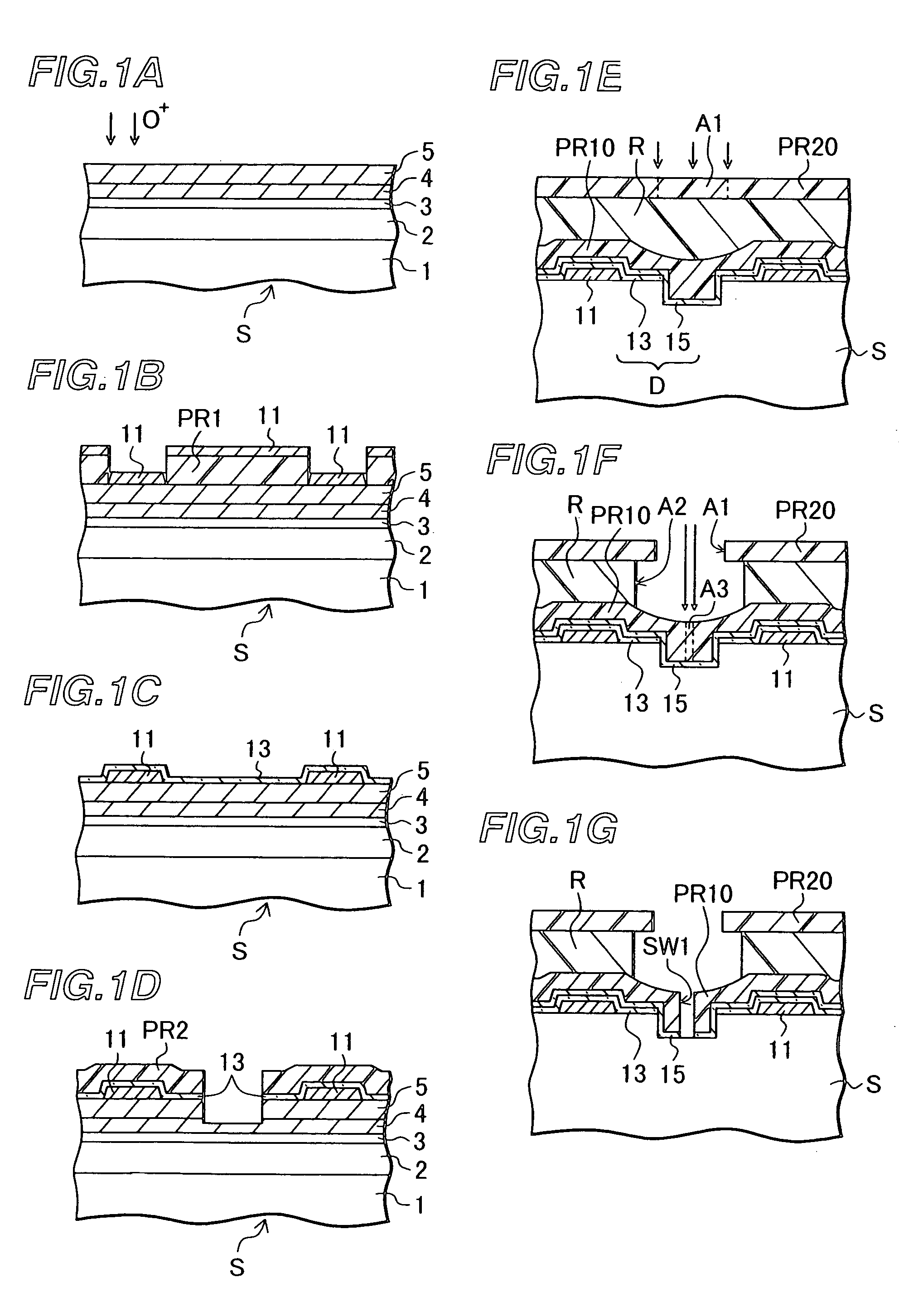
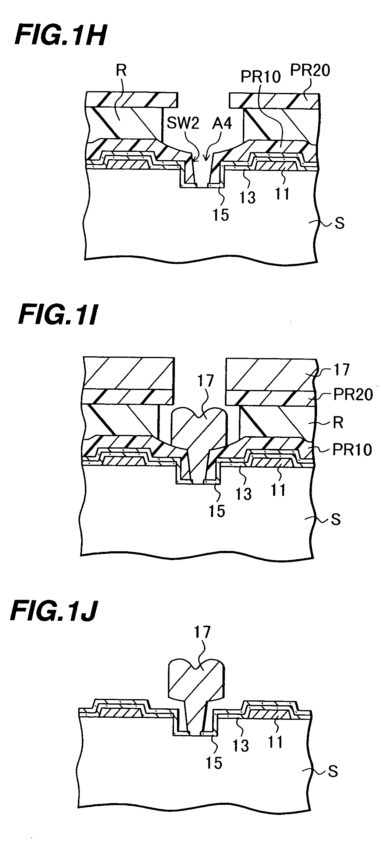
[0034]Prior to describing the embodiments of the invention, the study results made by the inventors will be described.

[0035]In order to form a fine mushroom gate electrode, it is desired to form an opening of an upwardly broadened taper shape in a resist layer. As resist capable of forming such an opening, polymethylmethacrylate (PMMA) is used by way of example.

[0036]As shown in FIG. 6A, on the surface of a semiconductor substrate 50, a resist layer 51 of PMMA is formed to a desired thickness by spin coating. Baking is performed at a temperature near the boiling point of resist solvent to evaporate the solvent. The resist layer 51 after baking is subjected to electron beam (EB) drawing and developed to form an opening 52 having generally vertical side walls.

[0037]As shown in FIG. 6B, as the developed resist layer 51 is subjected to heat treatment, the side wall of the opening 52 changes to have an upwardly broadening forward taper shape. A forward taper opening 52x is therefore obta...


PUM


Abstract

A semiconductor device has: a semiconductor substrate having a pair of current input / output regions via which current flows; an insulating film formed on the semiconductor substrate and having a gate electrode opening; and a mushroom gate electrode structure formed on the semiconductor substrate via the gate electrode opening, the mushroom gate electrode structure having a stem and a head formed on the stem, the stem having a limited size on the semiconductor substrate along a current direction and having a forward taper shape upwardly and monotonically increasing the size along the current direction, the head having a size expanded stepwise along the current direction, and the stem contacting the semiconductor substrate in the gate electrode opening and riding the insulating film near at a position of at least one of opposite ends of the stem along the current direction.

Description

CROSS REFERENCE TO RELATED APPLICATIONS[0001]This application is a Divisional or prior application Ser. No. 10 / 084, 924 filed Mar. 1, 2002 now U.S. Pat. No. 6,717,271 which is based on Japanese patent applications No. 2001-236301, filed on Aug. 3, 2001, and No. 2002-019361, filed on Jan. 29, 2002, the whole contents of which are incorporated herein by reference.BACKGROUND OF THE INVENTION[0002]A) Field of the Invention[0003]The present invention relates to a semiconductor device and its manufacture method, and more particularly to a semiconductor device having a so-called mushroom electrode and its manufacture method.[0004]B) Description of the Related Art[0005]The operation speed of a field effect transistor depends upon the gate length along the current path direction. In order to speed up a field effect transistor, it is desired to shorten the gate length. If the resistance of the gate electrode increases, a high speed operation of the transistor is restrained. In order to lower ...

Claims


Application Information

Patent Timeline
IPC IPC(8): H01L21/338H01L21/44H01L21/027H01L21/28H01L29/417H01L29/423H01L29/43H01L29/47H01L29/49H01L29/78H01L29/812H01L29/872
CPCH01L21/0274H01L21/28114H01L21/28264H01L21/28587H01L29/42316H01L29/42376H01L29/517H01L29/66462H01L29/66871H01L29/78Y10S430/143Y10S438/949Y10S438/951Y10S438/95
Inventor MAKIYAMA, KOZOIKECHI, NAOYATAN, TAKAHIRO
Owner FUJITSU LTD
Why Eureka
Try Eureka