Current source architecture for memory device standby current reduction

a memory device and current source architecture technology, applied in the field of memory devices, can solve the problems of data retention, additional circuits (e.g., charge pumps and the like) that may be necessary to generate the back-up, and may not be sufficient for smaller sized technologies, and achieve the effect of reducing the standby curren

Active Publication Date: 2007-06-05
INFINEON TECH LLC
View PDF10 Cites 35 Cited by
  • Summary
  • Abstract
  • Description
  • Claims
  • Application Information

AI Technical Summary

Benefits of technology

[0018]In such an arrangement, in a standby mode, data values within a memory cell block can be maintained according to a minimum current value, as opposed to a forced voltage value. This can allow for a lower standby current while not adversely affecting data retention properties
[0019]According to one aspect of the embodiments, a standby current source can comprise a p-channel metal-oxide-semiconductor field e

Problems solved by technology

As will be described below, while such an approach may be adequate for larger sized technologies and forgiving standby current values, such approaches may not be sufficient for smaller sized technologies and more stringent standby current specifications.
A drawback to such a conventional approach can be the additional circuits (e.g., charge pumps and the like) that may be necessary to generate the back-gate bias.
A drawback to such a conventional approach can be data retention.
This can result in loss/corruption of stored data values.
A drawback to such an approach can be the added complexity and/or cost necessary to provide such differ

Method used


Image

  • Current source architecture for memory device standby current reduction
  • Current source architecture for memory device standby current reduction
  • Current source architecture for memory device standby current reduction

Examples


first embodiment

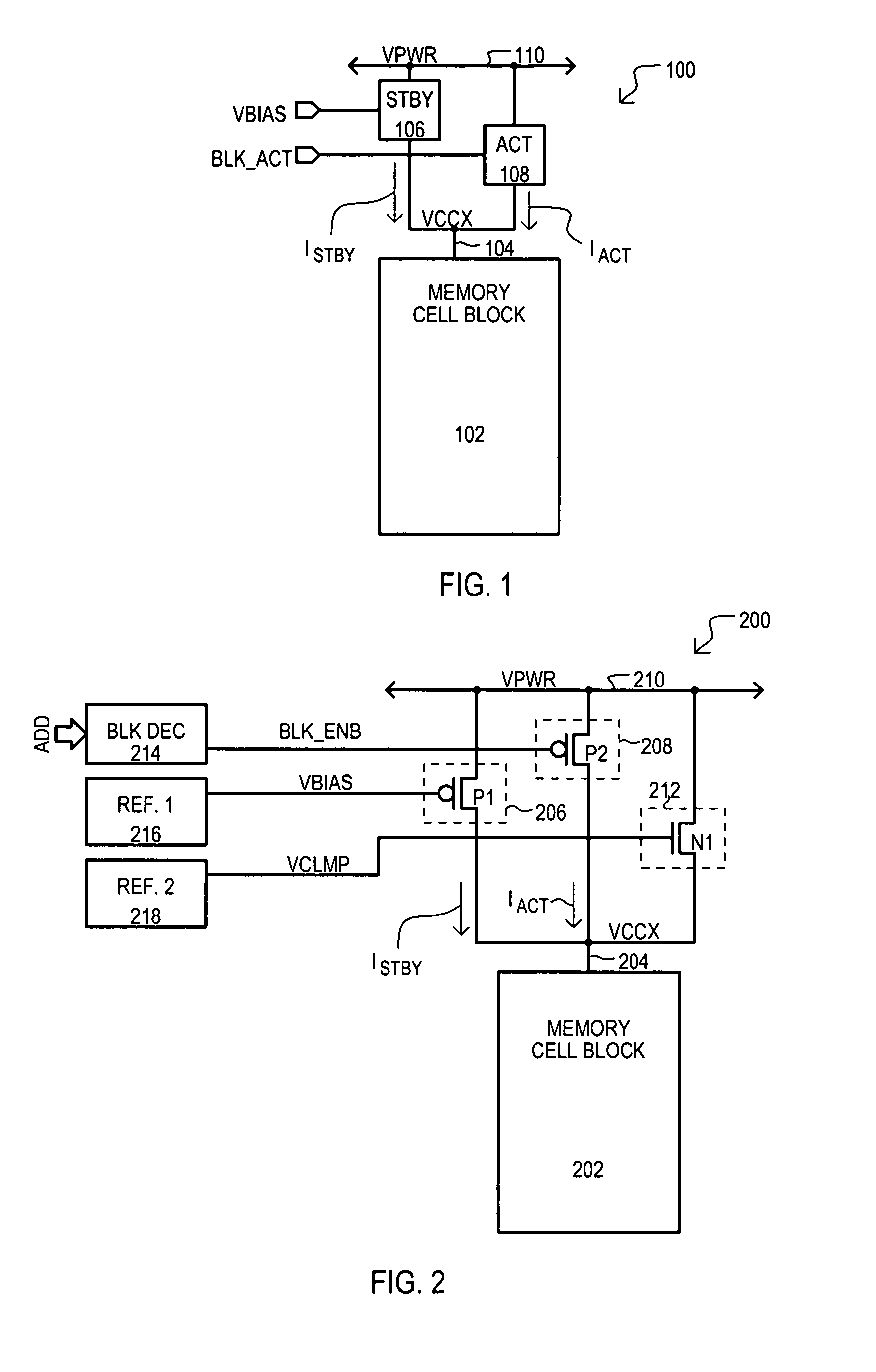
[0059]Referring now to FIG. 1, a memory device is set forth in a block schematic diagram and designated by the general reference character 100. A memory device 100 can include a memory cell block 102 with a number of memory cells. A memory cell block 102 can receive power at a block supply node 104.

[0060]A standby current source 106 and an active current source 108 can be situated between a power supply voltage node 110 and block supply node 104. An active current source 108 can provide an active current IACT in an active mode of operation (e.g., when memory cells are accessed for a read / write operation).

[0061]Standby current source 106 can provide a constant or regulated standby current ISTBY. Such a standby current ISTBY can be maintained at, or preferably above a minimum data retention current. It is understood that as a regulated current, ISTBY can be supplied to memory cell block 102 without regard to a voltage VCCX at supply node 104. In this way, the embodiment differs from ...

third embodiment

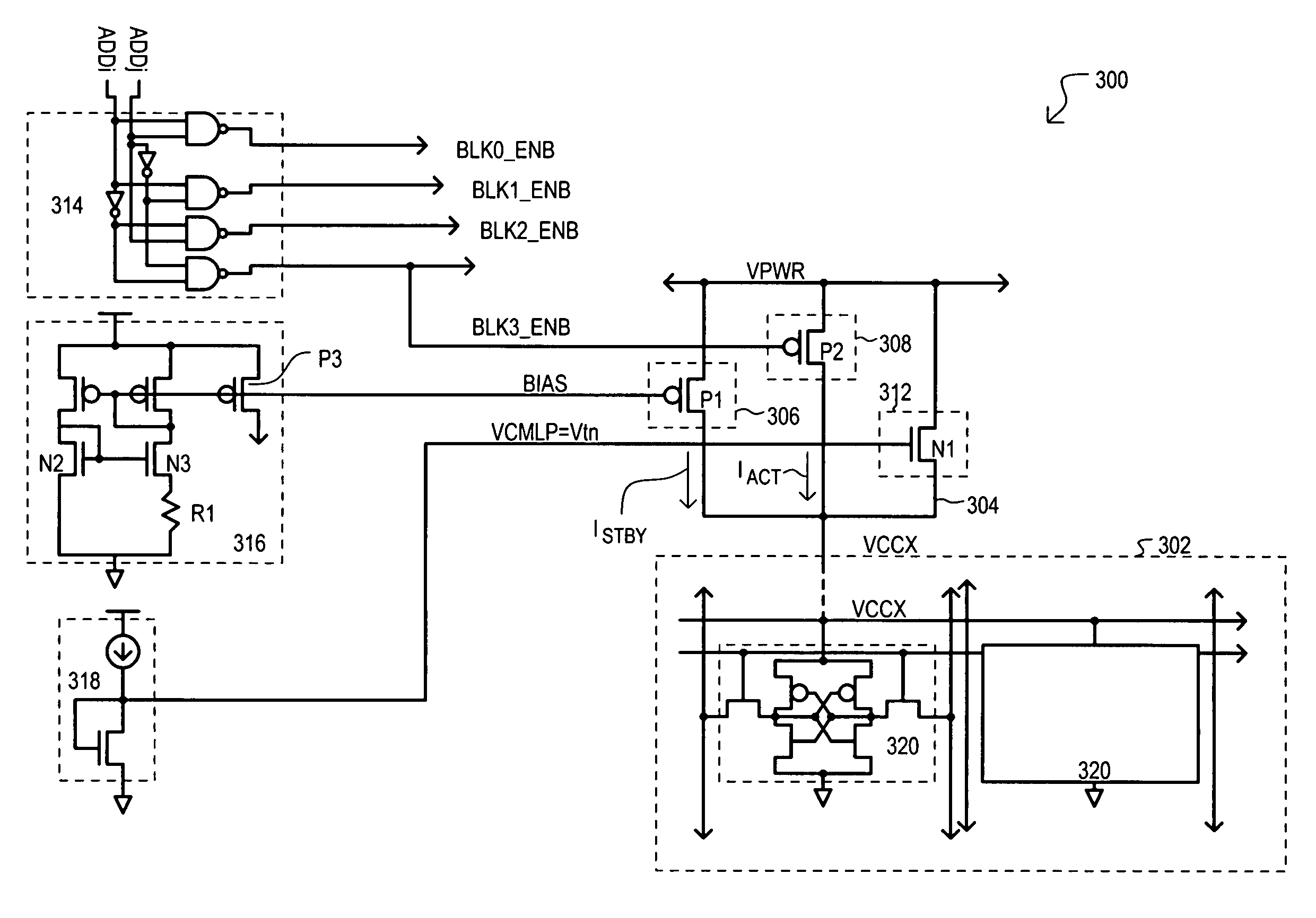
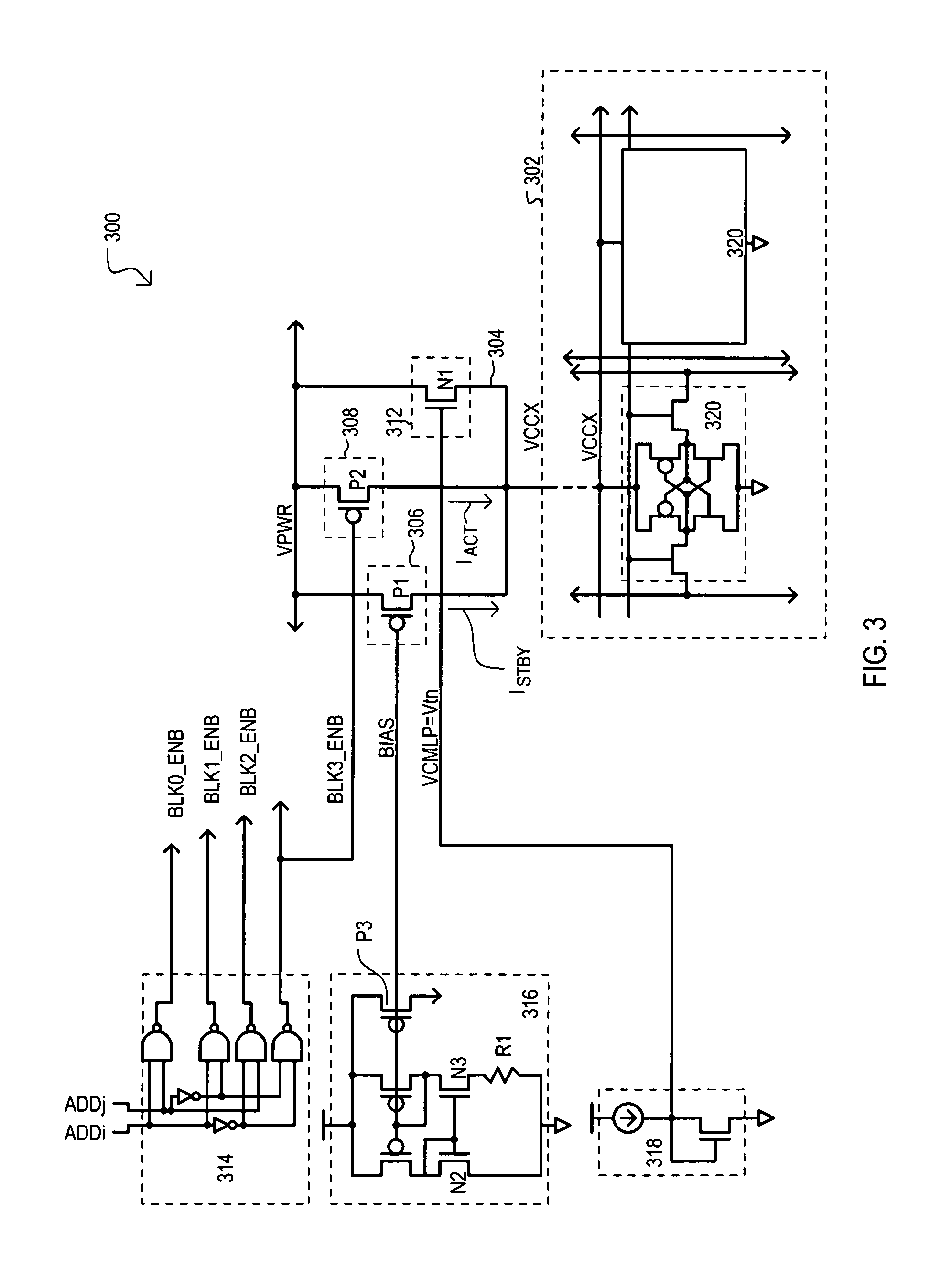
[0076]Referring now to FIG. 3, a memory device 300 is set forth in a detailed schematic diagram. FIG. 3 includes some of the same general sections as FIG. 2. Thus, like sections will be referred to by the same reference character but with the first digit being a “3” instead of a “2”.

[0077]In the example of FIG. 3, a memory cell block 302 may include six-transistor (6-T) type static random access memory (SRAM) cells 320 having p-channel device coupled to a block supply node 304. It is understood that the present invention should not necessarily be limited to any particular type of memory cell.

[0078]FIG. 3 also shows a particular type of a first reference circuit 316 and second reference circuit 318. A first reference circuit 316 can be a beta multiplier circuit that generates a reference current Iref that follows the relationship:

Iref=(nkT / Q)1n{m} / R

where kT / Q is the thermal voltage, m is the ratio between n-channel devices (N2 and N3) forming the current mirror within the reference...


PUM


Abstract

A memory device (200) can include a memory cell block (202), a standby current source (206), an active current source (208), and a clamping device (212). In a standby mode, a standby current source (206) can provide constant standby current ISTBY to memory cell block (202) via block supply node (204). In an active mode, active current source (208) can provide current to accommodate current necessary for active operations (e.g., accessing the memory cell block). A clamping circuit (212) can provide additional current in the event a block supply node (204) potential VCCX collapses due to the presence of micro-defects. In addition, compensation for process variation can be achieved by a self regulating well (454) to source (404) back bias that can modulate the threshold voltage of p-channel transistors of memory cells within the well (454), reducing overall leakage.

Description

TECHNICAL FIELD[0001]The present invention relates generally to memory devices, and more particularly to methods and circuits for reducing a standby current in a memory device.BACKGROUND OF THE INVENTION[0002]Many memory devices have both an active and standby mode. In an active mode, storage locations can be accessed according to a particular operation (e.g., read, write, program, erase, etc.). In a standby state, storage locations are typically not accessed, and a memory device retains the data values stored within.[0003]While it remains a continuing goal to reduce overall power consumption in memory devices, low power consumption can be a particularly important feature in limited power systems (e.g., battery powered devices). Such a need has given rise to low power memory devices, sometimes referred to as “micropower” or more battery life memory devices (including MoBL™ memory devices manufactured by Cypress Semiconductor Corporation of San Jose, Calif.).[0004]The particular memo...

Claims


Application Information

Patent Timeline
IPC IPC(8): G11C5/14
CPCG11C5/147G11C11/417
Inventor KOTHANDARAMAN, BADRINARAYANANMANN, ERICRODGERS, THURMAN J.
Owner INFINEON TECH LLC
Why Eureka
Try Eureka