Method of fabricating metal silicide layer

a technology of metal silicide layer and fabrication method, which is applied in the direction of basic electric elements, electrical apparatus, semiconductor devices, etc., can solve the problems of reducing the dimension of electronic devices, and reducing the resistance of electrical connection structures, so as to reduce the resistance and reduce the width of lines.

Active Publication Date: 2007-06-12
UNITED MICROELECTRONICS CORP
View PDF7 Cites 5 Cited by
  • Summary
  • Abstract
  • Description
  • Claims
  • Application Information

AI Technical Summary

Benefits of technology

[0009]Accordingly, at least one objective of the present invention is to provide a method of fabricating a metal silicide layer capable of minimizing the increase in resistance accompanied by a reduction of line width.
[0010]At least a second objective of the present invention is to provide a method of fabricating a metal silicide layer capable of removing the spiking problem in heavily doped P-type area and piping problem in heavily doped N-type area when using nickel silicide.
[0015]In the present invention, different types of metal silicide layers are formed on the substrate and the gate surface. This not only counteracts the increase in resistance due to a narrowing of the gate line width and the accompanied reduction in contact area between the metal silicide layer and the metallic interconnect above the gate, but also resolves spiking problem in the heavily doped P-type region and piping problem in the heavily doped N-type region when nickel silicide alone is used.

Problems solved by technology

However, as the dimension of an electronic device is reduced, a number of challenging problems is encountered in the process of fabricating the integrated circuits.
In particular, as devices continue to shrink in size, a reduction in the resistance of electrical connection structures has become increasingly important because any increase in the resistance will directly lead to a slow-down in the operating speed through an increase in RC delay.
However, the same problem is encountered when the line width is again reduced.

Method used


Image

  • Method of fabricating metal silicide layer
  • Method of fabricating metal silicide layer
  • Method of fabricating metal silicide layer

Examples


Embodiment Construction

[0020]Reference will now be made in detail to the present preferred embodiments of the invention, examples of which are illustrated in the accompanying drawings. Wherever possible, the same reference numbers are used in the drawings and the description to refer to the same or like parts.

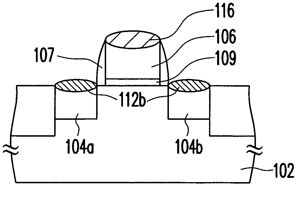
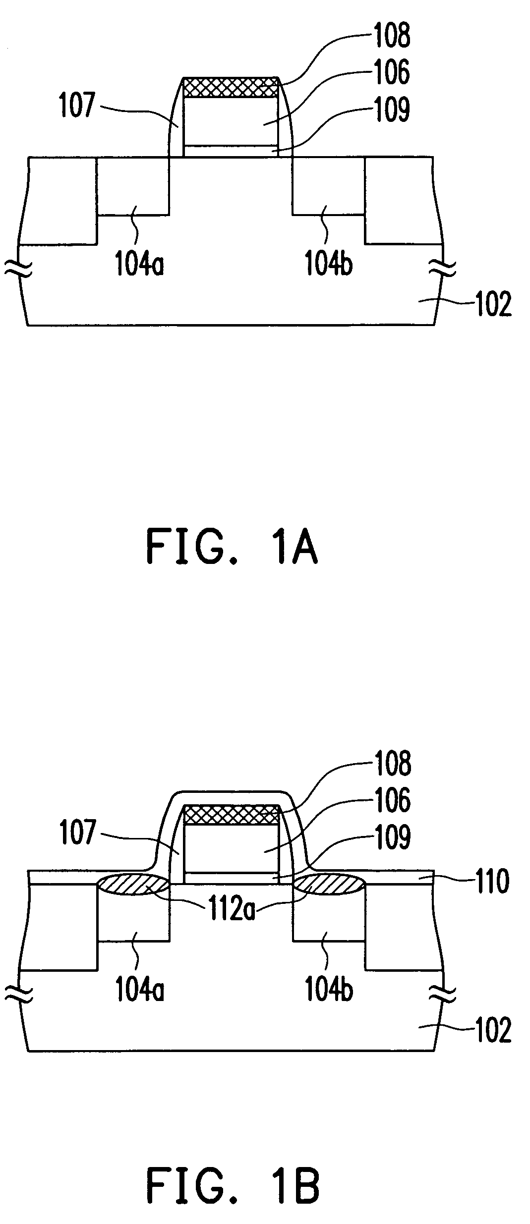
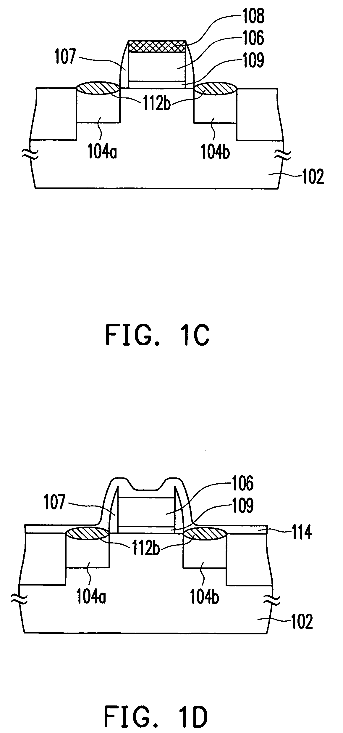
[0021]The concept behind the method of fabricating a metal silicide layer is to form one type of metal silicide layer over the source region and drain region of the substrate and another type of metal silicide layer over the gate. Hence, the high resistance problem in narrow gate lines and the spiking and piping problem in the source / drain regions for using nickel silicide are resolved at the same time. The following embodiment describes a few applications of the present invention and hence should be used to limit the scope of the present invention. In fact, the present invention can be applied to any semiconductor fabrication process that demands the deposition of a different type of metal silicide ...


PUM

PropertyMeasurementUnit
temperatureaaaaaaaaaa

Abstract

A method of fabricating a metal silicide layer over a substrate is provided. First, a hard mask layer is formed over a gate formed on a substrate and a portion of the substrate is exposed. Thereafter, a first metal silicide layer, which is a cobalt silicide or a titanium silicide layer, is formed on the exposed substrate. After that, the hard mask layer is removed and a second metal silicide layer is formed over the gate, wherein a material of the second metal silicide layer is selected from a group consisting of nickel silicide, platinum silicide, palladium silicide and nickel alloy. Since different metal silicide layers are formed on the substrate and the gate, the problem of having a high resistance in lines with a narrow line width and the problem of nickel silicide forming spikes and pipelines in the source region and the drain region are improved.

Description

BACKGROUND OF THE INVENTION[0001]1. Field of the Invention[0002]The present invention relates to a semiconductor processing method and structure thereof. More particularly, the present invention relates to a method of fabricating a metal silicide layer such that different metal silicide materials are formed on different crystalline regions of a substrate.[0003]2. Description of the Related Art[0004]In ultra-high level integration, the size of each semiconductor device is reduced so that the level of integration can continue to increase. After miniaturizing the electronic devices, the semiconductor integrated circuit can have the highest level of integration. However, as the dimension of an electronic device is reduced, a number of challenging problems is encountered in the process of fabricating the integrated circuits. In particular, as devices continue to shrink in size, a reduction in the resistance of electrical connection structures has become increasingly important because any...

Claims


Application Information

Patent Timeline
Patent Type & Authority Patents(United States)
IPC IPC(8): H01L21/44
CPCH01L21/28518H01L21/324H01L29/66507H01L29/78
Inventor CHEN, YI-WEIHUNG, TZUNG-YUCHIANG, YI-YIINGHSIEH, CHAO-CHINGCHANG, YU-LAN
Owner UNITED MICROELECTRONICS CORP
Why Eureka
Try Eureka