
Method of fabricating metal silicide layer
a technology of metal silicide layer and fabrication method, which is applied in the direction of basic electric elements, electrical apparatus, semiconductor devices, etc., can solve the problems of reducing the dimension of electronic devices, and reducing the resistance of electrical connection structures, so as to reduce the resistance and reduce the width of lines.
- Summary
- Abstract
- Description
- Claims
- Application Information
AI Technical Summary
Benefits of technology
Problems solved by technology
Method used
Image

Examples
Embodiment Construction
[0020] Reference will now be made in detail to the present preferred embodiments of the invention, examples of which are illustrated in the accompanying drawings. Wherever possible, the same reference numbers are used in the drawings and the description to refer to the same or like parts.
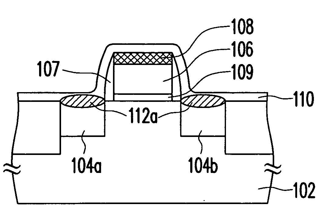
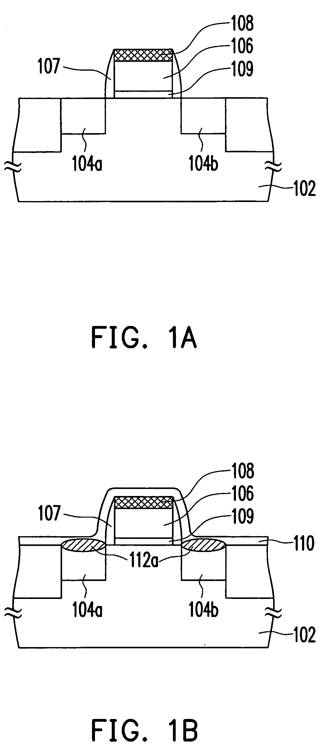
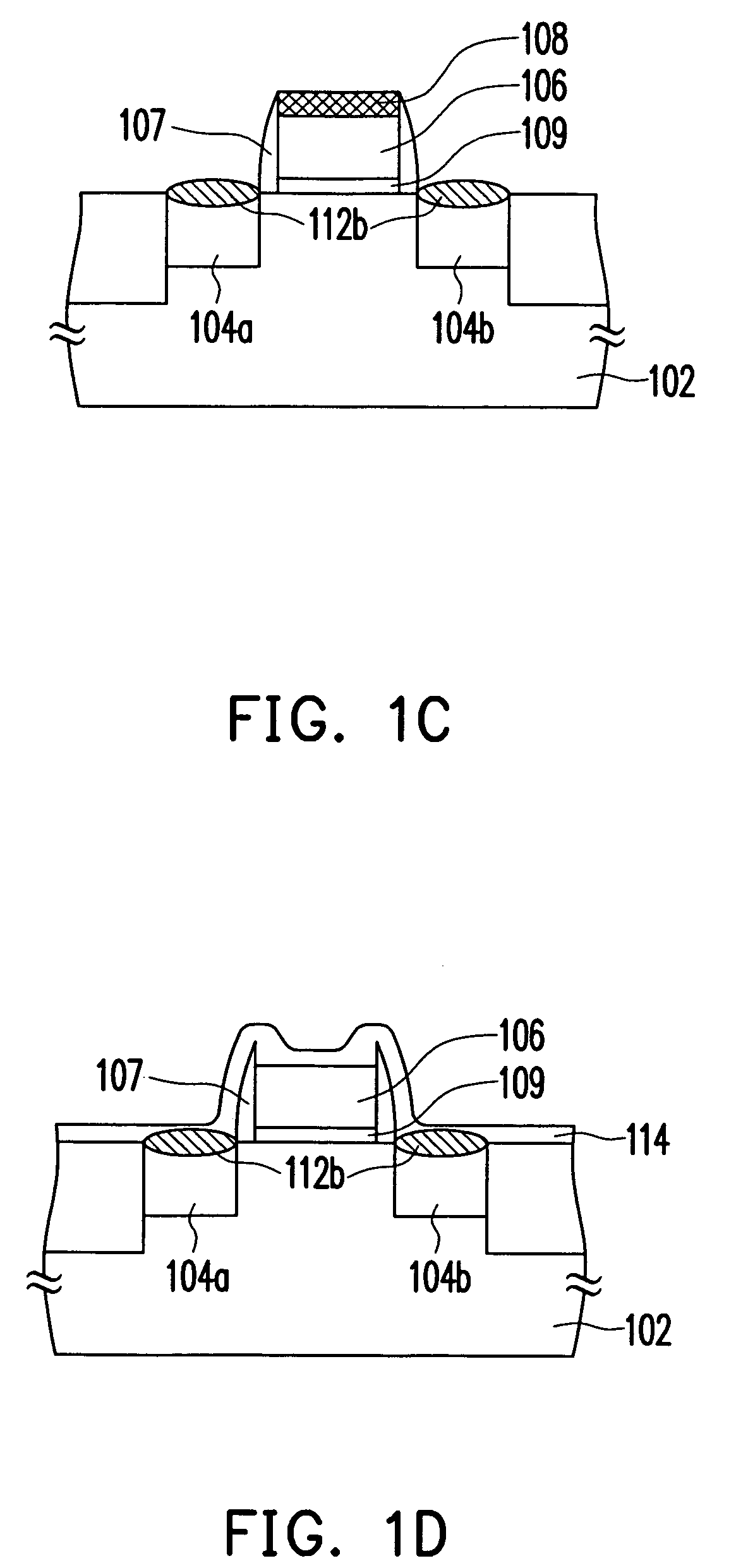
[0021] The concept behind the method of fabricating a metal silicide layer is to form one type of metal silicide layer over the source region and drain region of the substrate and another type of metal silicide layer over the gate. Hence, the high resistance problem in narrow gate lines and the spiking and piping problem in the source / drain regions for using nickel silicide are resolved at the same time. The following embodiment describes a few applications of the present invention and hence should be used to limit the scope of the present invention. In fact, the present invention can be applied to any semiconductor fabrication process that demands the deposition of a different type of metal silici...
PUM
| Property | Measurement | Unit |
|---|---|---|
| temperature | aaaaa | aaaaa |
| temperature | aaaaa | aaaaa |
| metallic | aaaaa | aaaaa |
Abstract
Description
Claims
Application Information