Semiconductor inspection system

a technology of semiconductors and inspection systems, applied in semiconductor/solid-state device testing/measurement, material analysis using wave/particle radiation, instruments, etc., can solve the problems of inability to accurately match, the registration of templates may incur a considerable decline in the entire throughput, and the inability to achieve accurate matching, etc., to achieve the effect of efficient decision

Inactive Publication Date: 2007-06-26
HITACHI LTD
View PDF16 Cites 49 Cited by
  • Summary
  • Abstract
  • Description
  • Claims
  • Application Information

AI Technical Summary

Benefits of technology

[0033]In the semiconductor inspection system according to the second aspect, the navigation system includes the function to design semiconductor patterns by itself or the function to retrieve and store the design information from another navigation system connected via a network which possesses a designing function. Therefore, the capturing and inspecting conditions can be readily set up based on the design information.
[0054]In the semiconductor inspection system according to the twenty-third aspect, in the case that a part of the capturing and inspecting conditions inside the capturing and inspecting condition file being registered in advance is modified and edited, the semiconductor inspection system of the nineteenth aspect is provided with a function to register the relevant condition with the capturing and inspecting condition file as another condition. Therefore the conditions can be efficiently decided thereafter.

Problems solved by technology

In actual measurement, frequent capturing operations for registration of the templates may incur a considerable decline in entire throughput.
Moreover, since technologies for matching design data with SEM images have not been developed adequately, accurate matching has been difficult to do.
For this reason, there has been a problem that throughput is not improved because registration is time-consuming and the system is occupied at the time of registration.
Moreover, there has been a problem that it is impossible to construct an operator-free and fully automated semiconductor inspection system because the conventional system always requires an operator for judgment and registration by observation of actual SEM images.
Furthermore, concerning the technology for matching design information with the SEM images, the conventional technology cannot respond to deformation between the CAD data and the SEM images.
The conventional technology also has a problem in the event of extracting edge information out of the SEM image that the edge information cannot be adequately extracted due to a signal / noise ratio (an S / N ratio) of the image.
In the event of generating a line image by conversion into binary codes, the conventional technology would be incapable of obtaining an optimum value for a threshold, because determination thereof has been difficult.
Accordingly, there has been a problem that a correlation coefficient becomes considerably small in the subsequent matching process by normalized correlation.

Method used


Image

  • Semiconductor inspection system
  • Semiconductor inspection system
  • Semiconductor inspection system

Examples


Embodiment Construction

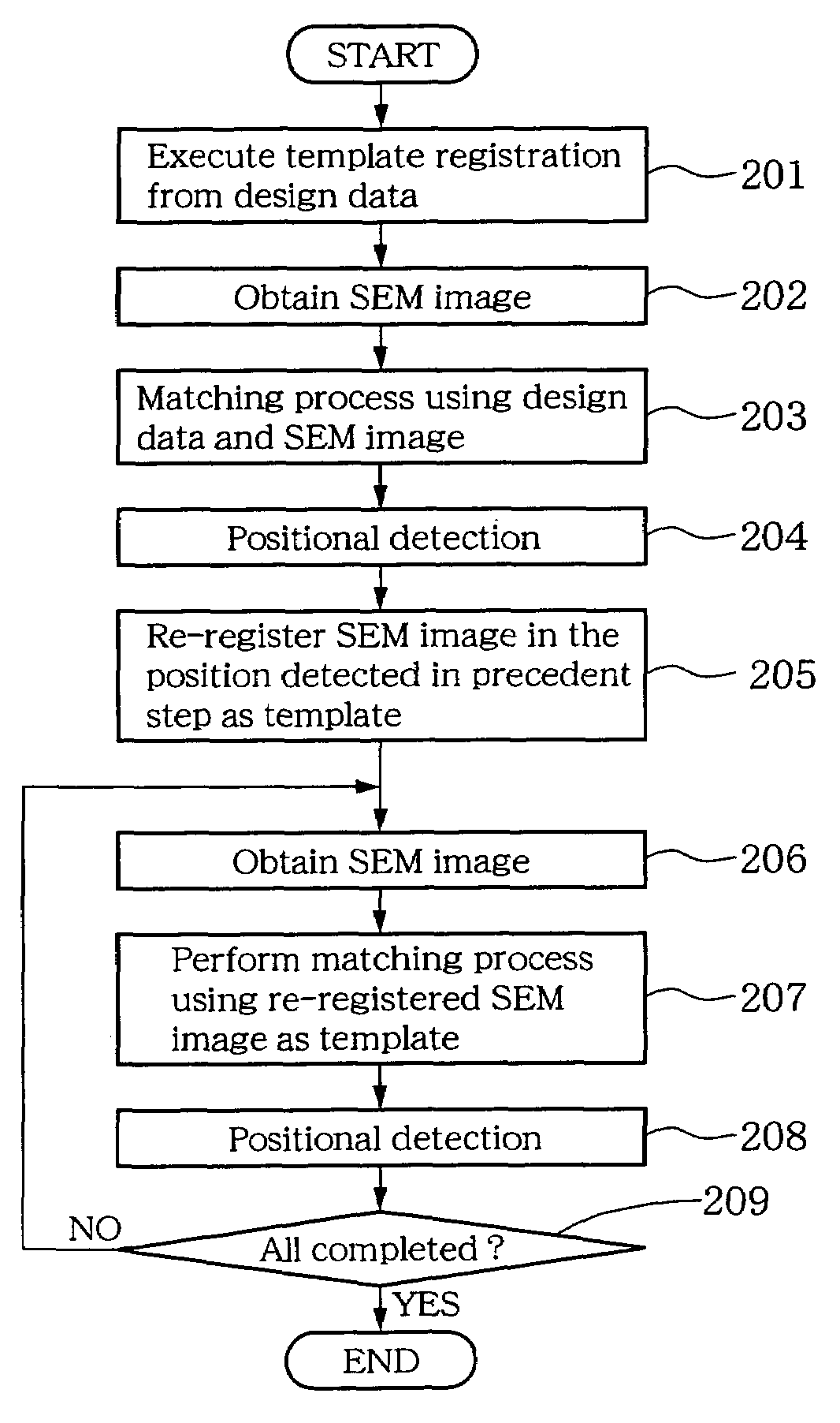
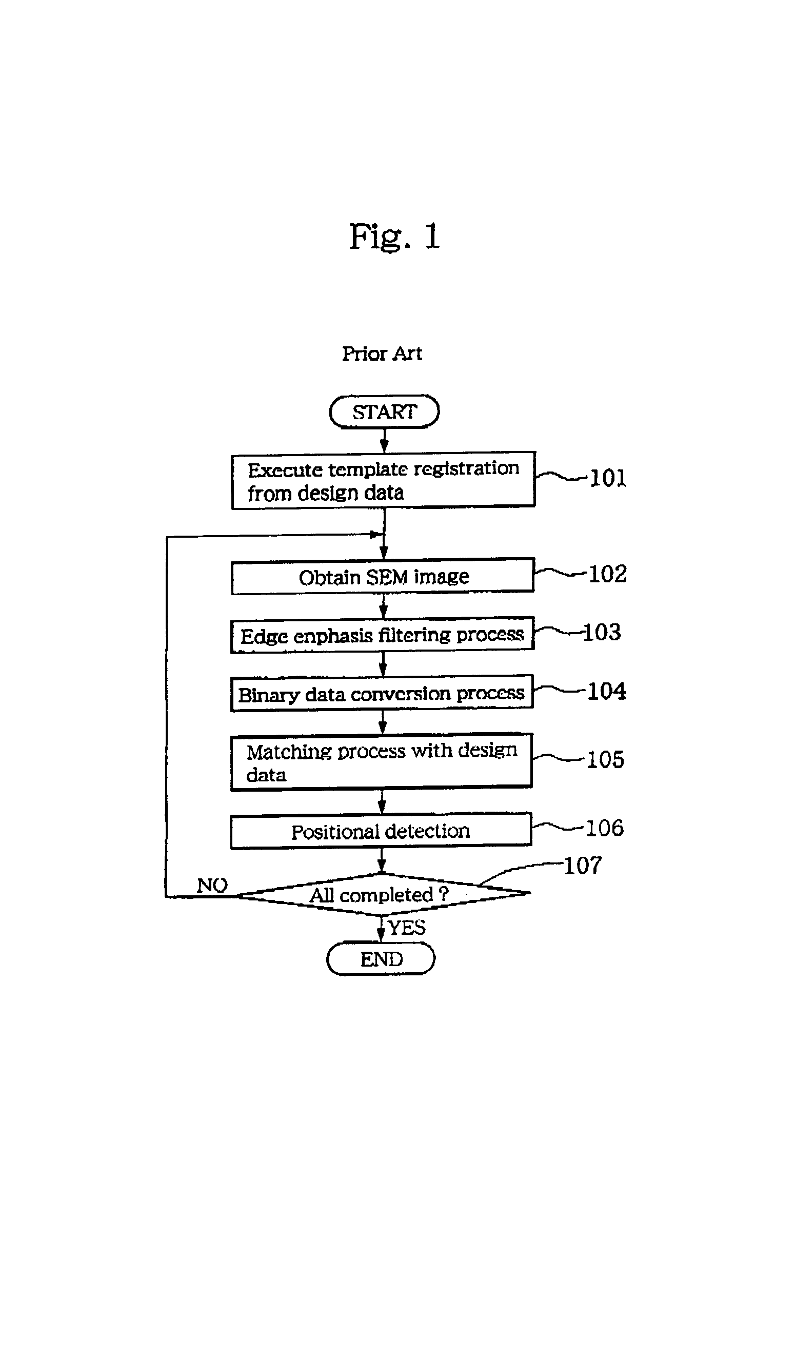
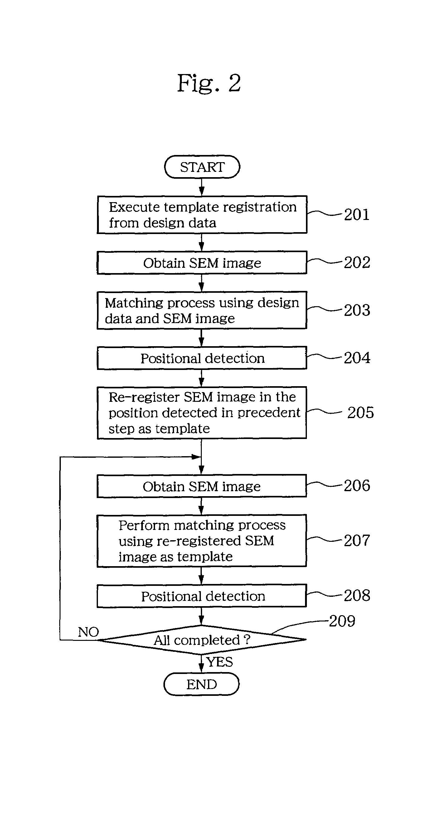
[0076]FIG. 3 is a block diagram of a schematic configuration of a scanning electron microscope system of the present invention. Reference numeral 301 denotes a body of an electron microscope. An electron beam 303 emitted out of an electron gun 302 is converged by an unillustrated electron lens and irradiated on a sample 305. Either intensity of secondary electrons generated from a surface of the sample or intensity of reflected electrons by electron beam irradiation is detected by an electron detector 306 and amplified by an amplifier 307. Reference numeral 304 denotes a deflector 304 which deflects the electron beam, thus subjecting the electron beam 303 to raster scanning on the sample surface according to a control signal 308 of a controlling computer 310. A signal outputted from the amplifier 307 is converted from analog to digital inside an imaging processor 309, whereby digital image data are generated. Reference numeral 311 denotes a display device for displaying the image da...


PUM

PropertyMeasurementUnit
sizeaaaaaaaaaa
scanning electron microscopeaaaaaaaaaa
grayscaleaaaaaaaaaa

Abstract

An operator-free and fully automated semiconductor inspection system with high throughput is realized. All conditions required for capturing and inspection are generated from design information such as CAD data. In order to perform actual inspection under the conditions, a semiconductor inspection system is composed of a navigation system for generating all the conditions required for capturing and inspection from the design information and a scanning electron microscope system for actually performing capturing and inspection. Moreover, in the case of performing a matching process between designed data and a SEM image, deformed parts are corrected by use of edge information in accordance with multiple directions and smoothing thereof. Furthermore, a SEM image corresponding to a detected position is re-registered as a template, and the matching process is thereby performed.

Description

BACKGROUND OF THE INVENTION[0001]1. Field of the Invention[0002]The present invention relates to a semiconductor inspection system for analyzing patterns on a semiconductor wafer by use of design data. More specifically, the present invention relates to a semiconductor inspection system provided with a system configuration for automatically generating conditions for capturing and inspection of patterns out of the design data, as well as a method of stably performing a matching process between the design data and scanning electron microscope (SEM) images.[0003]2. Background Art[0004]In recent years, there is a production shift in the semiconductor industry from production of memory chips to production of system large scale integrated circuits (LSIs). From a viewpoint of patterns on a semiconductor wafer, unlike patterns of a memory chip, patterns of a system LSI are not designed as simply repeated patterns. Accordingly, in the case of performing pattern measurement of the system LSI ...

Claims


Application Information

Patent Timeline
Patent Type & Authority Patents(United States)
IPC IPC(8): H01J37/28G01B15/00G01N23/225H01L21/66
CPCH01J37/28
Inventor TAKANE, ATSUSHIYODA, HARUOYOSHIDA, SHOJIIKEDA, MITSUJIOZAWA, YASUHIKO
Owner HITACHI LTD
Why Eureka
Try Eureka