System and method for integrating low schottky barrier metal source/drain

a metal source/drain, low schottky barrier technology, applied in the direction of semiconductor devices, electrical apparatus, transistors, etc., can solve the problems of low contact resistance, infinite abruptness, low contact resistance, etc., to reduce the schottky barrier height and reduce the barrier height

Active Publication Date: 2007-07-03
TEXAS INSTR INC
View PDF8 Cites 12 Cited by
  • Summary
  • Abstract
  • Description
  • Claims
  • Application Information

AI Technical Summary

Benefits of technology

[0005]Embodiments of the invention provide a number of technical advantages. Embodiments of the invention may include all, some, or none of these advantages. According to one embodiment, the conduction band offset of strained silicon reduces the Schottky barrier height between N inversion layer and metal silicide. For NMOS, where highly strained silicon and ErSi is used, zero barrier height may be formed. For PMOS, with a thin strained silicon layer, the holes like to conduct in the SiGe layer, which has a valence band offset and reduces the barrier height between the P inversion layer and metal silicide. If PtSi is used, then the barrier height may be reduced to zero. Such integration schemes allows the full metal source / drain MOSFETs to be fabricated with readily available metal silicides.

Problems solved by technology

Metal source / drain offers lower sheet resistance than doped silicon, possesses infinite abruptness, and exhibits low contact resistance.
No such metals or metal silicides currently exist to achieve this.

Method used


Image

  • System and method for integrating low schottky barrier metal source/drain
  • System and method for integrating low schottky barrier metal source/drain
  • System and method for integrating low schottky barrier metal source/drain

Examples


Embodiment Construction

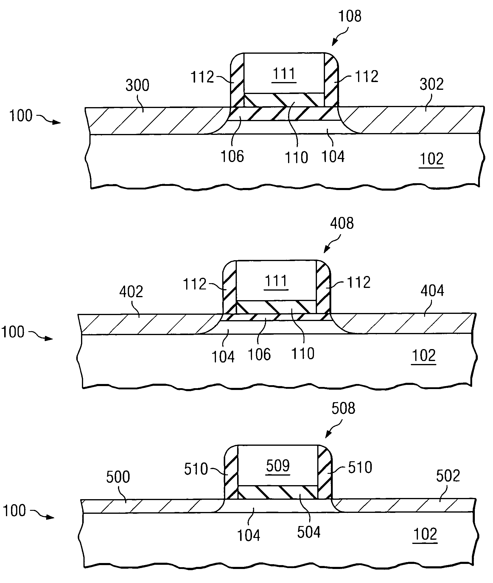
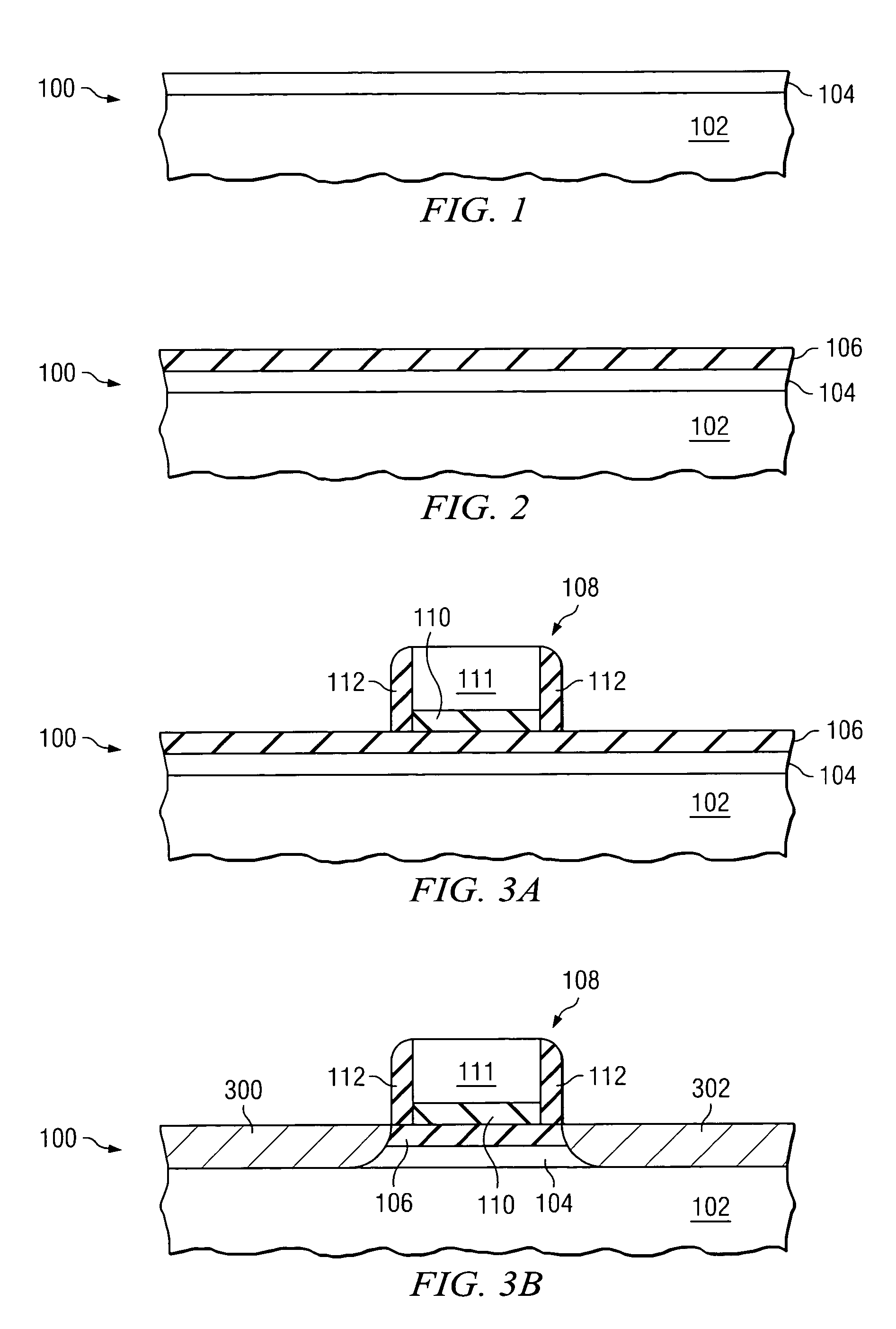
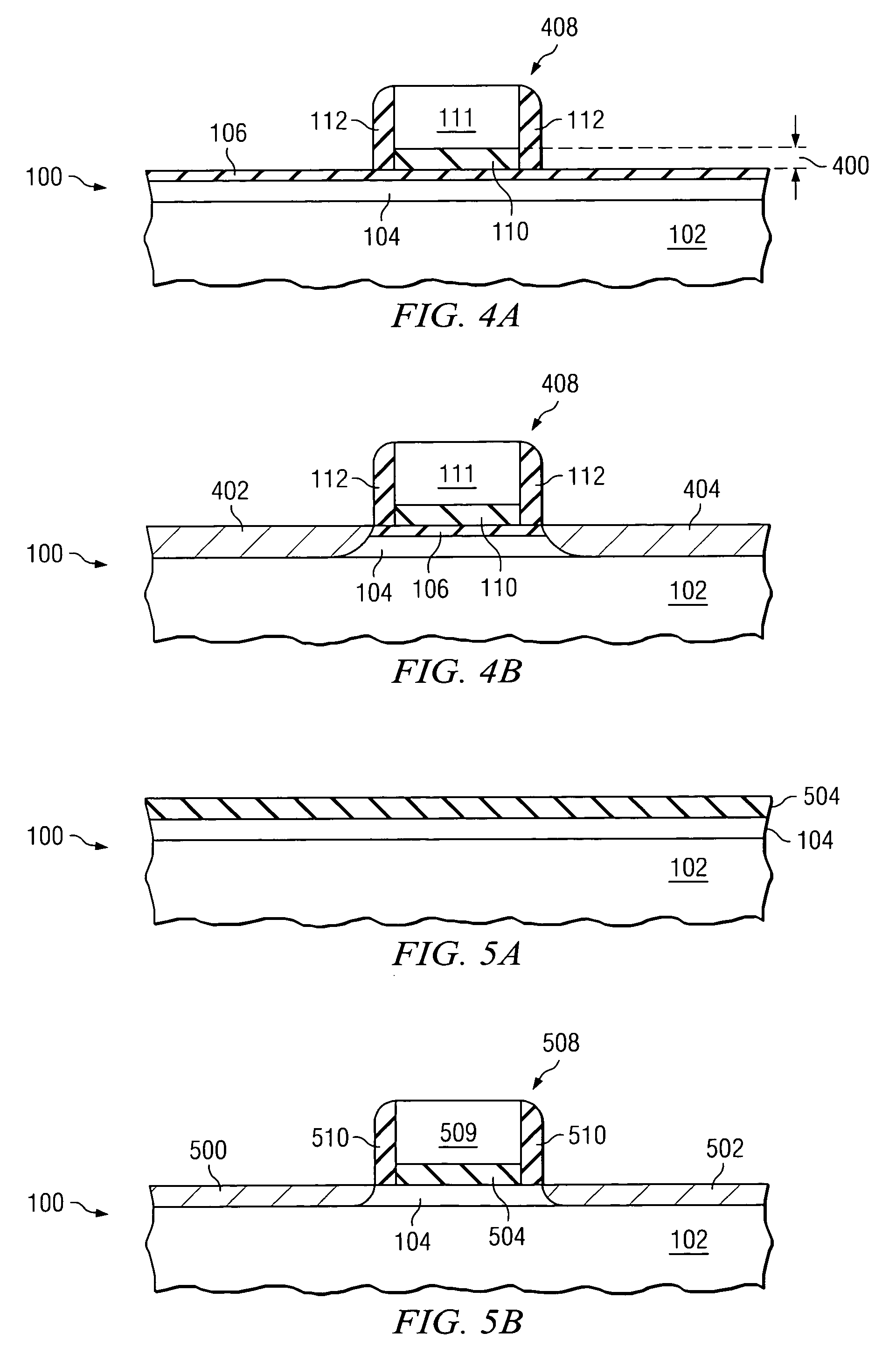
[0012]Example embodiments of the present invention and their advantages are best understood by referring now to FIGS. 1 through 5B of the drawings, in which like numerals refer to like parts.

[0013]FIGS. 1 and 2 are a series of cross-sectional views illustrating various manufacturing stages of a partially-completed MOSFET 100 in accordance with some embodiments of the present invention. MOSFET 100, as used throughout this detailed description, represents a partially-completed MOSFET integrated in a CMOS device, such as an NMOS, PMOS, or other suitable semiconductor device. In the embodiment illustrated in FIGS. 1 and 2, MOSFET 100 includes a substrate 102, a silicon germanium (“SiGe”) layer 104 formed outwardly from substrate 102, and a silicon layer 106 formed outwardly from the SiGe layer 104.

[0014]Substrate 102 may be formed from any suitable semiconductor materials, such as silicon and germanium and may have any suitable crystal orientation. The present invention is particularly ...


PUM

PropertyMeasurementUnit
structureaaaaaaaaaa
thicknessaaaaaaaaaa
depthaaaaaaaaaa

Abstract

According to one embodiment of the invention, a method for integrating low Schottky barrier metal source / drain includes providing a substrate, forming an epitaxial SiGe layer outwardly from the substrate, forming an epitaxial Si layer outwardly from the SiGe layer, and forming a metal source and a metal drain.

Description

TECHNICAL FIELD OF THE INVENTION[0001]The present invention relates generally to the field of semiconductor devices and, more particularly, to a system and method for integrating low Schottky barrier metal source / drain.BACKGROUND OF THE INVENTION[0002]Semiconductor manufacturers have recently been experimenting with metal source / drain MOSFETs. Metal source / drain offers lower sheet resistance than doped silicon, possesses infinite abruptness, and exhibits low contact resistance. In addition, there is no issue with random doping effect from source / drain to the channel. Lower cost due to the elimination of implanters and fancy annealing tools is also a driver.[0003]However, for metal source / drain to work, the Schottky barrier height between the metal and conducting channel in the silicon should be close to zero for acceptable drive current. No such metals or metal silicides currently exist to achieve this. Currently, ErSi and PtSi have the lowest barrier height, but the barrier height ...

Claims


Application Information

Patent Timeline
Patent Type & Authority Patents(United States)
IPC IPC(8): H01L21/8242
CPCH01L29/1054H01L29/66643H01L29/78H01L29/78687
Inventor XIONG, WEIZE
Owner TEXAS INSTR INC
Why Eureka
Try Eureka