Schottky Electrode of Nitride Semiconductor Device and Process for Production Thereof

a technology of nitride semiconductor and gate electrode, which is applied in the direction of semiconductor devices, basic electric elements, electrical apparatus, etc., can solve the problems of large reverse leak current, low barrier height of schottky gate electrode, etc., and achieves fine electrode shape, inhibits a decrease in schottky barrier height, and suppresses piezoelectric charge

Inactive Publication Date: 2008-01-10
NEC CORP
View PDF0 Cites 1 Cited by
  • Summary
  • Abstract
  • Description
  • Claims
  • Application Information

AI Technical Summary

Benefits of technology

[0029] The present invention provides a Schottky electrode for a nitride semiconductor which has a layered structure that comprises a copper (Cu) layer being in contact with the nitride semiconductor and a first electrode material layer formed on the copper (Cu) layer as an upper layer thereof, wherein such material that has a thermal expansion coefficient smaller than that of Cu and such a threshold temperature at which it starts to undergo a solid phase reaction with Cu being 400° C. or higher is selected as the first electrode material.
[0030] As the thermal expansion coefficient of the first electrode material is smaller than the thermal expansion coefficient of Cu, it has such an effect of suppressing a piezoelectric charge generated by deformation of the nitride semiconductor and of inhibiting a decrease in a Schottky barrier height resulting from generation of the piezoelectric charge. Furthermore, a solid phase reaction of the first electrode material with Cu is hardly induced by a heat treatment at 300° C. or higher and 650° C. or lower, and thus, it also has an effect of maintaining a fine electrode shape.

Problems solved by technology

In a nitride semiconductor electric field effect transistor, a metal multilayer film structure including Ni, Pt and Pd has been previously used as a Schottky electrode material (JP 10-223901 A, JP 11-219919 A and JP 2004-087740 A), but there has been such a problem that a Schottky gate electrode made therewith exhibits such a low barrier height of about 0.9 to 1.0 eV and a large reverse leak current.

Method used


Image

  • Schottky Electrode of Nitride Semiconductor Device and Process for Production Thereof
  • Schottky Electrode of Nitride Semiconductor Device and Process for Production Thereof
  • Schottky Electrode of Nitride Semiconductor Device and Process for Production Thereof

Examples


first embodiment

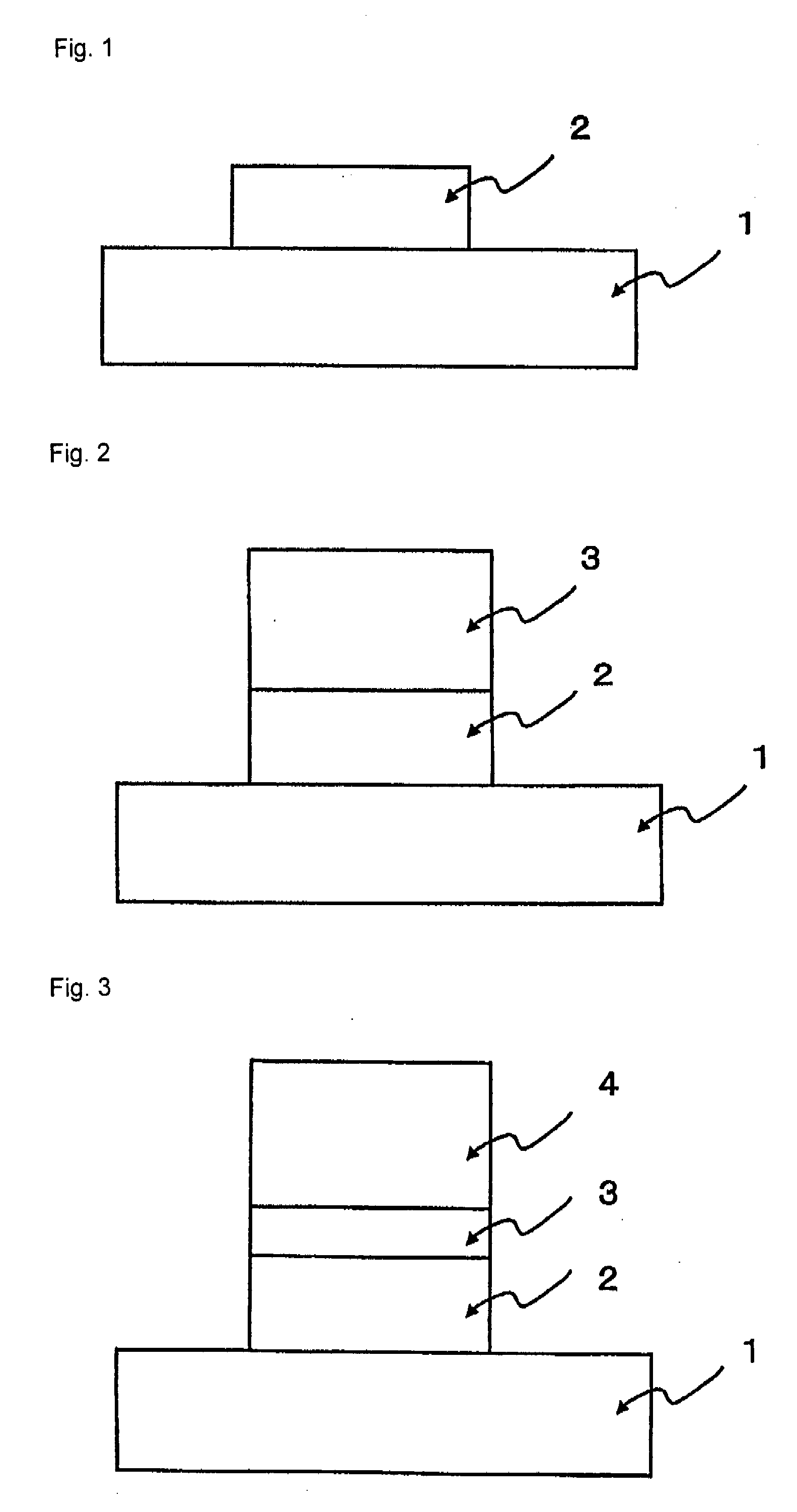
[0044] One embodiment according to the present invention is illustrated in FIG. 1. FIG. 1 shows a sectional view of a Schottky electrode for a nitride semiconductor device as the first embodiment according to the present invention.

[0045] As shown in FIG. 1, copper (Cu) layer 2 is formed on the surface of a nitride semiconductor 1. By increasing the thickness of the copper (Cu) layer 2 formed therefor, the gate resistance can be reduced, whereby a high-output transistor operating at a high frequency can be realized. Further, it is confirmed that a heat treatment at such a temperature as 300° C. or 400° C. in the production process of the element has the effect of increasing a barrier height and reducing a gate leak current.

example 1

[0046] This embodiment will be explained below by referring to a specific example. As a nitride semiconductor layer 1, an AlN buffer layer having a thickness of 4 nm and an n type GaN layer having a donor concentration of 1017 atoms·cm−3 and a thickness of 2000 nm were formed on a high-resistance SiC substrate. Furthermore, Ti and Al were successively deposited thereon as an ohmic electrode for the nitride semiconductor. Thereafter, it was subjected to a heat treatment at 650° C. in a nitrogen atmosphere to form an ohmic contact.

[0047] After that, copper (Cu) 2 was deposited in a thickness of 200 nm or 400 nm and then lifted off to form a Schottky electrode according to the present invention. The Schottky electrode could also be formed by means of sputtering. Furthermore, for comparison, samples of conventional type in which Ni / Au, Pt / Au or Pd / Au was employed as electrode material were prepared. Table 1 shows the results measured for the samples.

[0048] [Table 1]

TABLE 1Electrode ma...

second embodiment

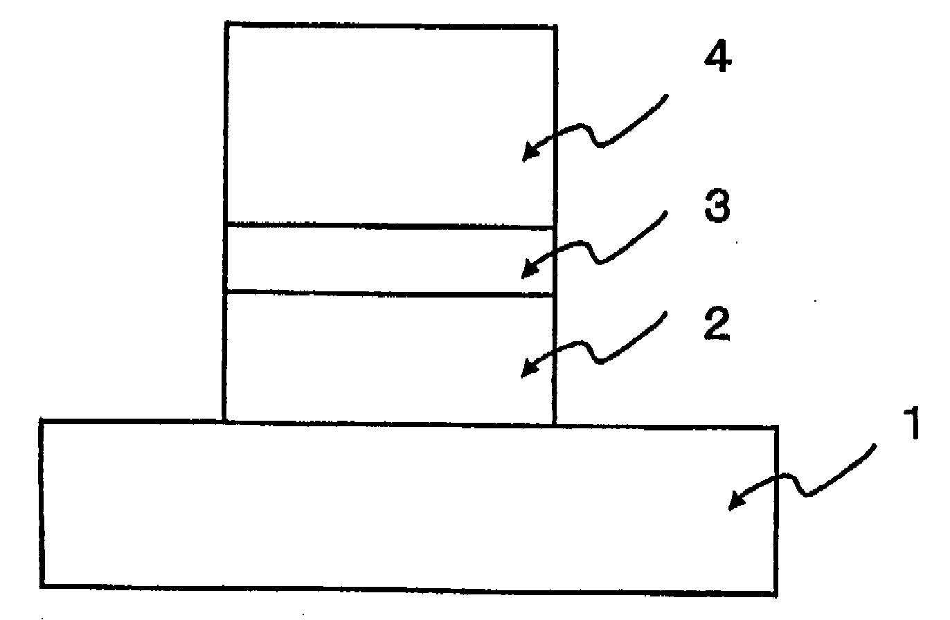
[0053] The second embodiment according to the present invention is illustrated in FIG. 2. FIG. 2 shows a sectional structure view of the second embodiment. This embodiment is a Schottky electrode which has a high barrier height, and allows the thickness to be increased so as to have a low resistance value.

[0054] A copper (Cu) 2 layer having a thickness of 200 nm is formed on the surface of a nitride semiconductor 1, and then, as an upper layer thereof, a molybdenum (Mo) layer is formed as a layer of a first electrode material 3. If this structure is used, a total thickness of the metal film formed can be thicker by means of a layered structure in which molybdenum (Mo) layer is formed as the upper layer, and therefore a gate resistance can be reduced, thus making it possible to realize a high-output transistor operating at a high frequency. Further, it has been found in test process for producing the element that a heat treatment at 300° C. to 400° C. has a similar effect of improvi...


PUM

PropertyMeasurementUnit
temperatureaaaaaaaaaa

Abstract

The present invention provides a Schottky electrode for a nitride semiconductor device having a high barrier height, a low leak current performance and a low resistance and being thermally stable, and a process for production thereof. The Schottky electrode for a nitride semiconductor has a layered structure that comprises a copper (Cu) layer being in contact with the nitride semiconductor and a first electrode material layer formed on the copper (Cu) layer as an upper layer. As the first electrode material, a metal material which has a thermal expansion coefficient smaller than the thermal expansion coefficient of copper (Cu) and starts to undergo a solid phase reaction with copper (Cu) at a temperature of 400° C. or higher is employed.

Description

TECHNICAL FIELD [0001] The present invention relates to a Schottky electrode for a nitride semiconductor device and a process for production thereof, and relates particularly to a Schottky electrode for a nitride semiconductor device which has a high barrier height, a low leak current performance and a low resistance and being thermally stable, and a process for production thereof. BACKGROUND ART [0002] In a nitride semiconductor electric field effect transistor, a metal multilayer film structure including Ni, Pt and Pd has been previously used as a Schottky electrode material (JP 10-223901 A, JP 11-219919 A and JP 2004-087740 A), but there has been such a problem that a Schottky gate electrode made therewith exhibits such a low barrier height of about 0.9 to 1.0 eV and a large reverse leak current. [0003] As an approach for solving the problem, there has been proposed use of copper (Cu) as a Schottky electrode material. According to TWHM 2003 proceedings (Topical Workshop on Hetero...

Claims


Application Information

Patent Timeline
Patent Type & Authority Applications(United States)
IPC IPC(8): H01L29/47H01L21/283H01L29/812
CPCH01L29/2003H01L29/812H01L29/475
Inventor MIYAMOTO, HIRONOBUNAKAYAMA, TATSUOANDO, YUJIOKAMOTO, YASUHIROKUZUHARA, MASAAKIINOUE, TAKASHIHATAYA, KOJI
Owner NEC CORP
Why Eureka
Try Eureka