Semiconductor device manufacturing method

A manufacturing method and semiconductor technology, applied in the fields of semiconductor/solid-state device manufacturing, semiconductor devices, electric solid-state devices, etc., can solve the problems of low temperature, poor solubility, and MOSFET cannot effectively reduce SBH, etc., so as to improve driving ability and improve solid solution degree, the effect of reducing the height of the Schottky barrier

Active Publication Date: 2013-06-05
INST OF MICROELECTRONICS CHINESE ACAD OF SCI
View PDF3 Cites 1 Cited by
  • Summary
  • Abstract
  • Description
  • Claims
  • Application Information

AI Technical Summary

Problems solved by technology

[0007] However, the above-mentioned method of using SADS to reduce SBH still has disadvantages: the solubility of the impurity ions injected into the source and drain 3A of the nickel-based metal silicide is very poor, and a large amount of implanted ions cannot be solid-dissolved in the nickel-based metal silicide, so it can be used for reducing The amount of doping ions in SBH is insufficient; the implanted ions diffuse through the grain boundary to segregate at the interface between the nickel-based metal silicide and silicon to form a coagulation region 7, but the temperature used for driving annealing is low enough to fully activate the segregation Impurities, the effect of reducing SBH is not significant
[0008] In short, the existing MOSFET cannot effectively reduce the SBH, thereby effectively reducing the source-drain resistance and effectively improving the device driving capability, which seriously affects the electrical performance of the semiconductor device, so there is an urgent need for a semiconductor device and its manufacturing method that can effectively reduce the SBH

Method used


Image

  • Semiconductor device manufacturing method
  • Semiconductor device manufacturing method
  • Semiconductor device manufacturing method

Examples


Embodiment Construction

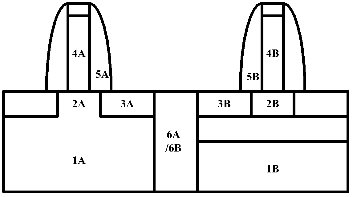
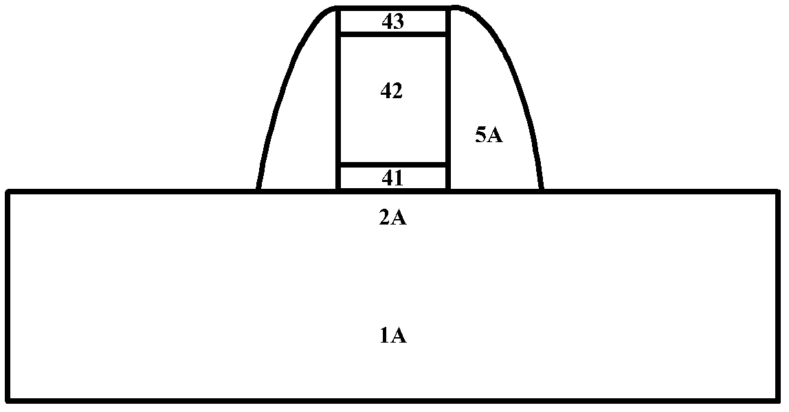
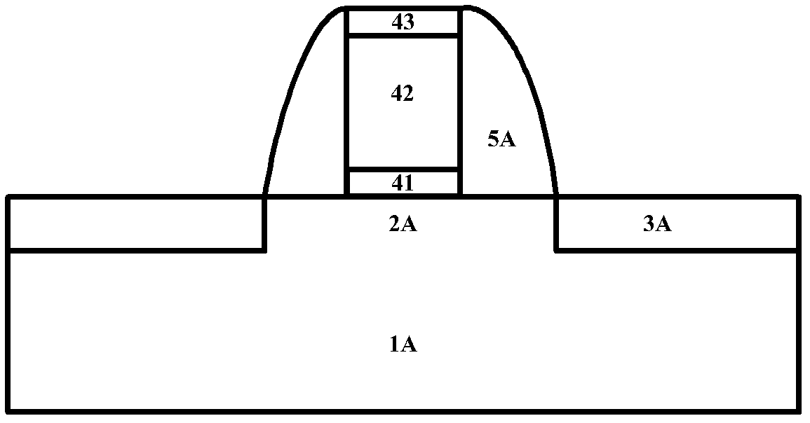
[0025] The features and technical effects of the technical solution of the present invention will be described in detail below with reference to the accompanying drawings and in conjunction with exemplary embodiments, and a semiconductor device capable of effectively reducing SBH and a manufacturing method thereof are disclosed. It should be pointed out that similar reference numerals represent similar structures, and the terms "first", "second", "upper", "lower" and the like used in this application can be used to modify various device structures or manufacturing processes . These modifications do not imply spatial, sequential or hierarchical relationships of the modified device structures or fabrication processes unless specifically stated.

[0026] First, as attached image 3 As shown, the substrate and gate basic structures are formed. For the embodiments of the present invention, conventional semiconductor substrates may be used, for example, may include bulk silicon su...


PUM

PropertyMeasurementUnit
thicknessaaaaaaaaaa

Abstract

The invention discloses a semiconductor device manufacturing method which comprises the steps of forming a grid stack structure on a substrate containing silicon; depositing nickel metal layers on the substrate and the grid stack structure; primarily annealing to enable silicon in the substrate to react with the nickel metal layer to form nickel-rick phase metal silicide; injecting ions to enable doping ions to be injected into the nickel-rich phase metal silicide; secondarily annealing to enable the nickel-rick phase metal silicide to be converted into nickel metal silicide source leakage and simultaneously forming separation and condensation zone at the interface between the nickel metal silicide source leakage and the substrate. According to the semiconductor device manufacturing method, doping ions are injected into the nickel-rick phase metal silicide to be annealed, solid solubility of the doping ions is improved to form the high-concentration doping ion separation and condensation zone, schottky barrier height between the nickel metal silicide and a silicon channel is effectively reduced, and driving capacity of the device is improved.

Description

technical field [0001] The invention relates to a semiconductor device manufacturing method, in particular to a MOSFET manufacturing method capable of effectively reducing the Schottky barrier height between metal silicide and silicon. Background technique [0002] As traditional MOSFET devices continue to be scaled down, the source-drain resistance does not decrease proportionally with the channel size reduction, especially the contact resistance increases approximately square times with the size reduction, which reduces the equivalent operating voltage and greatly affects the proportionality. shrinking device performance. If the traditional highly doped source / drain is replaced by metal silicide source and drain in the existing MOSFET manufacturing technology, the parasitic series resistance and contact resistance can be greatly reduced. [0003] Such as figure 1 As shown, it is a schematic diagram of an existing metal silicide source / drain MOSFET (also known as a Schott...

Claims


Application Information

Patent Timeline
Patent Type & Authority Applications(China)
IPC IPC(8): H01L21/336H01L21/28H01L21/265
CPCH01L21/283H01L21/28H01L27/1207H01L29/7833H01L29/66477H01L29/6659H01L21/28097H01L29/66772H01L29/665
Inventor 罗军赵超钟汇才李俊峰陈大鹏
Owner INST OF MICROELECTRONICS CHINESE ACAD OF SCI
Why Eureka
Try Eureka