Method of forming fin-type field effect transistor

A fin-type field effect and transistor technology, which is applied in semiconductor/solid-state device manufacturing, electrical components, circuits, etc., can solve the problems of transistor performance to be improved, and achieve the effect of uniform aluminum ion concentration distribution and high thickness uniformity

Active Publication Date: 2017-05-31
SEMICON MFG INT (SHANGHAI) CORP +1
View PDF3 Cites 1 Cited by
  • Summary
  • Abstract
  • Description
  • Claims
  • Application Information

AI Technical Summary

Problems solved by technology

[0004] The performance of the existing fin field effect transistors still needs to be improved

Method used


Image

  • Method of forming fin-type field effect transistor
  • Method of forming fin-type field effect transistor
  • Method of forming fin-type field effect transistor

Examples


Embodiment Construction

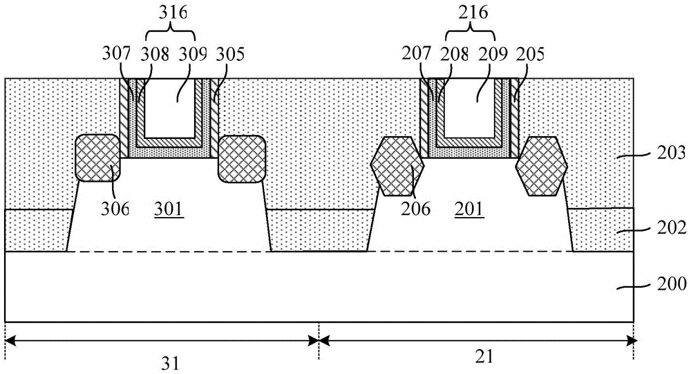
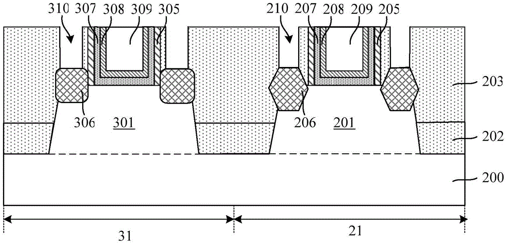
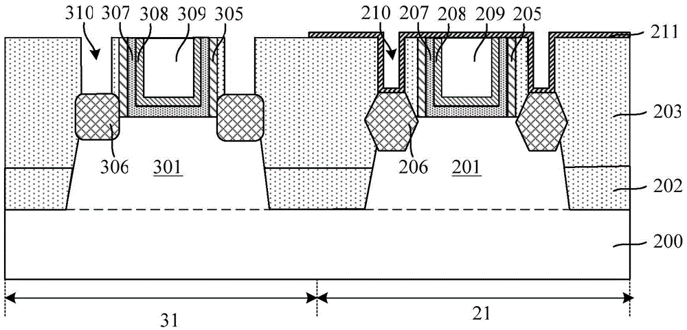
[0029] As mentioned in the background technology, the performance of the existing fin field effect transistor still needs to be improved. For example, the resistance of the metal silicide formed in the source region and the drain region of the fin field effect transistor formed in the prior art is still relatively large. The Schottky Barrier Height (Schottky Barrier Height, SBH) is still large, affecting the performance of the FinFET.

[0030] To this end, an embodiment of the present invention provides a method for forming a Fin Field Effect Transistor. A semiconductor substrate is provided, the semiconductor substrate includes an NMOS region and a PMOS region, and a first fin is formed on the semiconductor substrate of the NMOS region. portion, across the first gate covering the sidewall and top surface of the first fin, and the first source region and the first drain region in the first fin located on both sides of the first gate, the semiconductor substrate of the PMOS regi...


PUM

PropertyMeasurementUnit
Thicknessaaaaaaaaaa

Abstract

A method of forming a fin-type field effect transistor comprises: forming a first etch hole that exposes a first source region and a first drain region surface in a dielectric layer, and a second etch hole exposing a second source region and a second drain region; forming a second oxide layer containing aluminum on the side wall and the bottom surface of the second etch hole; forming a first oxide layer containing sulfur or selenium on the side wall and the bottom surface of the first etch hole; performing annealing such that sulfur ions or selenium ions in the first oxide layer containing sulfur or selenium diffuse into the first source region and the first drain region at the bottom of the first etch hole, aluminum ions in the second oxide layer containing aluminum diffuse into the second source region and the second drain region at the bottom of the second etch hole; and removing the first oxide layer and the second oxide layer, forming a first metal silicide on the surfaces of the first source region and the first drain region, and forming a second metal silicide layer on the surfaces of the second source region and the second drain region. The method of the present invention reduces the Schottky barrier height of the fin-type field effect transistor source-drain region.

Description

technical field [0001] The invention relates to the field of semiconductor manufacturing, in particular to a method for forming a fin field effect transistor. Background technique [0002] In the present invention, with the continuous development of semiconductor process technology, the process node is gradually reduced, and the gate-last process is widely used to obtain an ideal threshold voltage and improve device performance. However, when the feature size (CD, Critical Dimension) of the device is further reduced, even if the gate-last process is adopted, the structure of the conventional MOS field effect transistor can no longer meet the requirements for device performance, and the fin field effect transistor (Fin FET) as Substitution of conventional devices has received extensive attention. [0003] A method for forming a Fin Field Effect Transistor in the prior art includes: providing a semiconductor substrate on which protruding fins are formed, and the fins are gene...

Claims


Application Information

Patent Timeline
IPC IPC(8): H01L21/8238
CPCH01L21/823821H01L21/823871
Inventor 谢欣云徐建华
Owner SEMICON MFG INT (SHANGHAI) CORP
Why Eureka
Try Eureka