Versatile system for self-aligning deposition equipment

a self-aligning, equipment technology, applied in the direction of transportation and packaging, vacuum evaporation coating, coating, etc., can solve the problems of many traditional semiconductor fabrication techniques and processes rendered impractical or unusable, and conventional deposition techniques are simply not capable of depositing semiconductor material at sub-micron levels or tolerances, so as to improve process efficiency, yield and reliability, the effect of improving efficiency and accuracy

Active Publication Date: 2007-07-03
TEXAS INSTR INC
View PDF3 Cites 5 Cited by
  • Summary
  • Abstract
  • Description
  • Claims
  • Application Information

AI Technical Summary

Benefits of technology

[0009]The present invention provides a versatile system, comprising a number of apparatus and methods, for providing self-aligning deposition equipment and apparatus—such as thin-film deposition showerheads. The system of the present invention provides accurate and consistent equipment alignment, while obviating the need for iterative alignment processes. Subjective inconsistencies and errors inherent in conventional methodologies are removed by the present invention—replaced by standardized system, apparatus and procedures. By the present invention, the process of aligning deposition equipment is optimized for efficiency and accuracy, improving process efficiency, yield and reliability in an easy and cost-effective manner.
[0010]The system of the present invention accurately and reproducibly aligns or levels a first, adjustable apparatus with respect to a second, stationary apparatus. A standardized spacing or offset component is placed or secured along an operational surface of the stationary apparatus during alignment procedures. The spacing component is formed or assembled of a dimension or configuration corresponding to the desired or required operational offset between the adjustable apparatus and the stationary apparatus—thereby defining a proper alignment position for the adjustable apparatus.

Problems solved by technology

The increased packing density of the integrated circuit generates numerous challenges to the semiconductor manufacturing process.
As device geometries and features continually decrease in size, and as new materials are introduced into semiconductor fabrication processes, many traditional semiconductor fabrication techniques and processes are rendered impractical or unusable.
Some conventional deposition techniques are simply not capable of depositing semiconductor material at sub-micron levels or tolerances.
This is important because non-uniformities in thin-film materials can cause a number of variances in device performance or reliability, degrading process yields.
In many cases, however, showerheads frequently fall out of alignment during processing.
This routine process interruption introduces a significant degree of delay and inefficiency into fabrication processes utilizing such apparatus.
Such inefficiencies and delays are further compounded and increased by a number of impediments inherent in conventional showerhead alignment methodologies.
Most such systems require numerous iterations (e.g., 6, 8, 12) of laborious and tedious manual measurements and calibrations—each of which may take several hours, individually.
These manual adjustment procedures thus frequently take many (e.g., ˜12 or more) hours and, in some cases, days to complete—as the deposition system is repetitively operated, measured and adjusted until proper alignment is achieved.
This causes a number of bottlenecks in the fabrication process, and places an inordinate drain on other process resources.
This introduces, to at least a minimal extent, some degree of human error and unavoidable incongruity to the thin film deposition process.
Non-uniformities that result over time can have further detrimental impacts on process yields and stability.

Method used


Image

  • Versatile system for self-aligning deposition equipment
  • Versatile system for self-aligning deposition equipment
  • Versatile system for self-aligning deposition equipment

Examples


Embodiment Construction

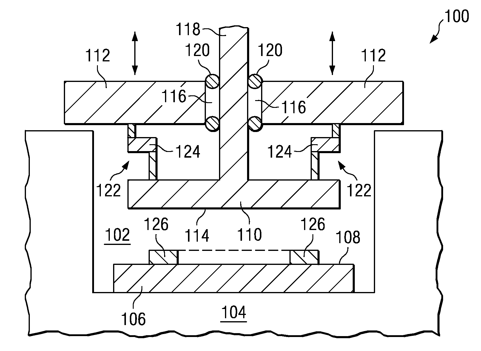
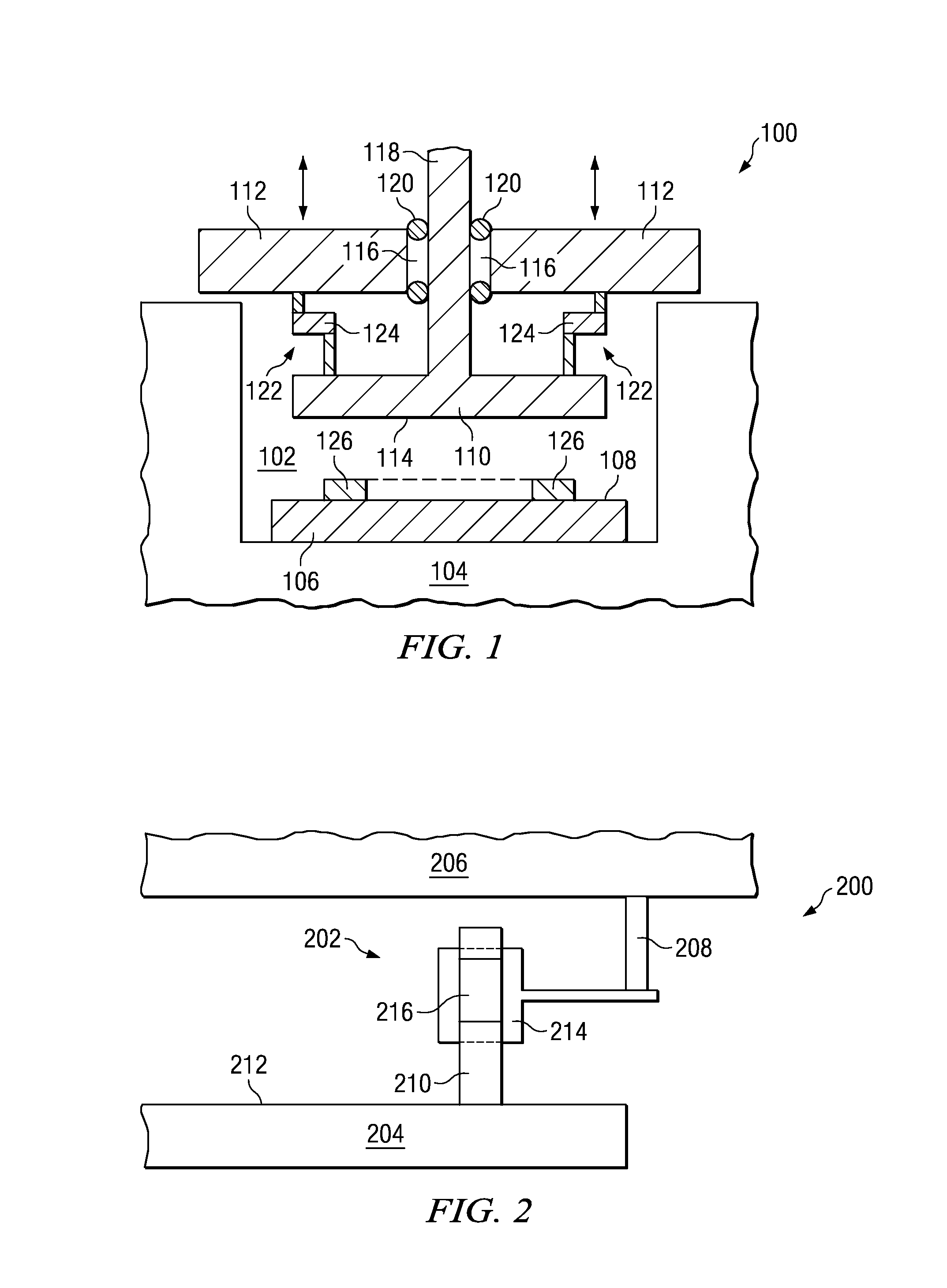
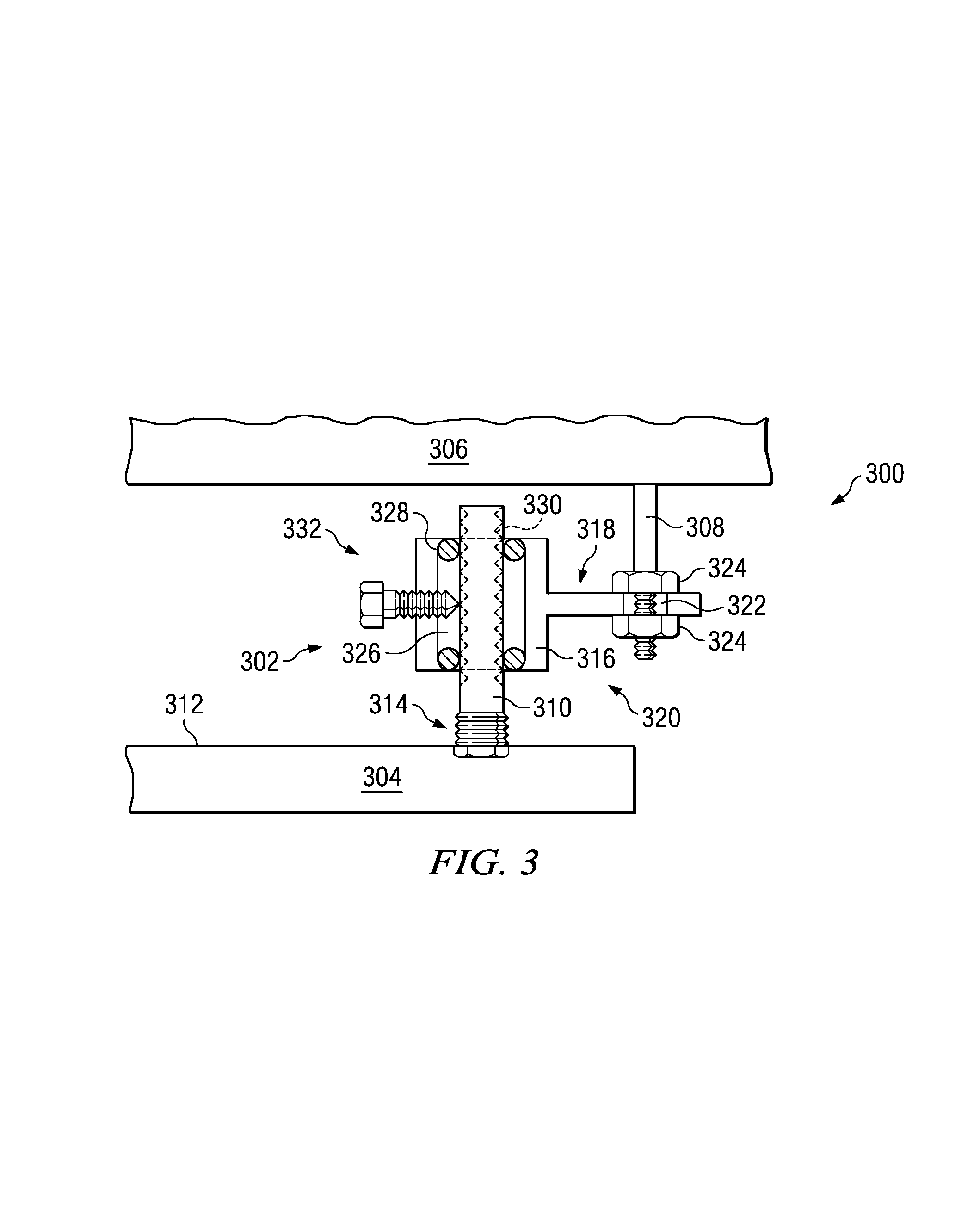
[0018]While the making and using of various embodiments of the present invention are discussed in detail below, it should be appreciated that the present invention provides many applicable inventive concepts, which can be embodied in a wide variety of specific contexts. Certain aspects of the present invention, for example, are hereafter illustratively described in specific conjunction with embodiments of self-aligning showerhead apparatus within thin-film deposition systems. The specific embodiments discussed herein are, however, merely demonstrative of specific ways to make and use the invention and do not limit the scope of the invention.

[0019]The present invention provides a versatile system that accurately and reproducibly aligns, adjusts, or levels (hereafter “aligns”) an adjustable apparatus with respect to a second, stationary apparatus. The present invention provides a standardized spacing or offset component that is placed or secured along an operational surface of the sta...


PUM

PropertyMeasurementUnit
temperatureaaaaaaaaaa
pressureaaaaaaaaaa
frictionaaaaaaaaaa

Abstract

The present invention provides a system (100) for aligning a dispensing apparatus (110) utilized within a semiconductor deposition chamber (102). A stationary reference apparatus (106) is disposed along the bottom of the deposition chamber. A self-alignment support system (122), comprising one or more support components (124), is intercoupled between the dispensing apparatus and a deposition system exterior component (112). The self-alignment support system is adapted to facilitate and secure repositioning of the dispensing apparatus responsive to pressure applied to the dispensing surface (114) thereof. A non-yielding offset component (126) is placed upon a first surface (108) of the stationary reference apparatus. The dispensing surface of the dispensing apparatus is engaged with the offset component, and pressure is applied to the dispensing apparatus via the offset component until a desired alignment is achieved.

Description

TECHNICAL FIELD OF THE INVENTION[0001]The present invention relates generally to the field of manufacturing semiconductor devices and, more particularly, to apparatus and methods for providing self-aligning deposition equipment.BACKGROUND OF THE INVENTION[0002]The continual demand for enhanced integrated circuit performance has resulted in, among other things, a dramatic reduction of semiconductor device geometries, and continual efforts to optimize the performance of every substructure within any semiconductor device. A number of improvements and innovations in fabrication processes, material composition, and layout of the active circuit levels of a semiconductor device have resulted in very high-density circuit designs. Increasingly dense circuit design has not only improved a number of performance characteristics, it has also increased the importance of, and attention to, semiconductor material properties and behaviors.[0003]The increased packing density of the integrated circuit...

Claims


Application Information

Patent Timeline
Patent Type & Authority Patents(United States)
IPC IPC(8): H01L21/31
CPCC23C16/45565C23C16/52H01L21/68H01L21/02104H01L21/6715Y10T29/49895C23C14/24C23C14/541
Inventor GARCIA, MARTIN
Owner TEXAS INSTR INC
Why Eureka
Try Eureka