

Process for manufacturing electrically conductive components
a manufacturing process and technology for electrically conductive components, applied in the field of forming electrode arrays, can solve the problems of difficult or impossible time-consuming, and the manufacture of wiring and connector components is often labour-intensive and specialised crafts. , to achieve the effect of reducing the pitting in the sheet and minimizing the pitting
- Summary
- Abstract
- Description
- Claims
- Application Information
AI Technical Summary
Benefits of technology
Problems solved by technology
Method used
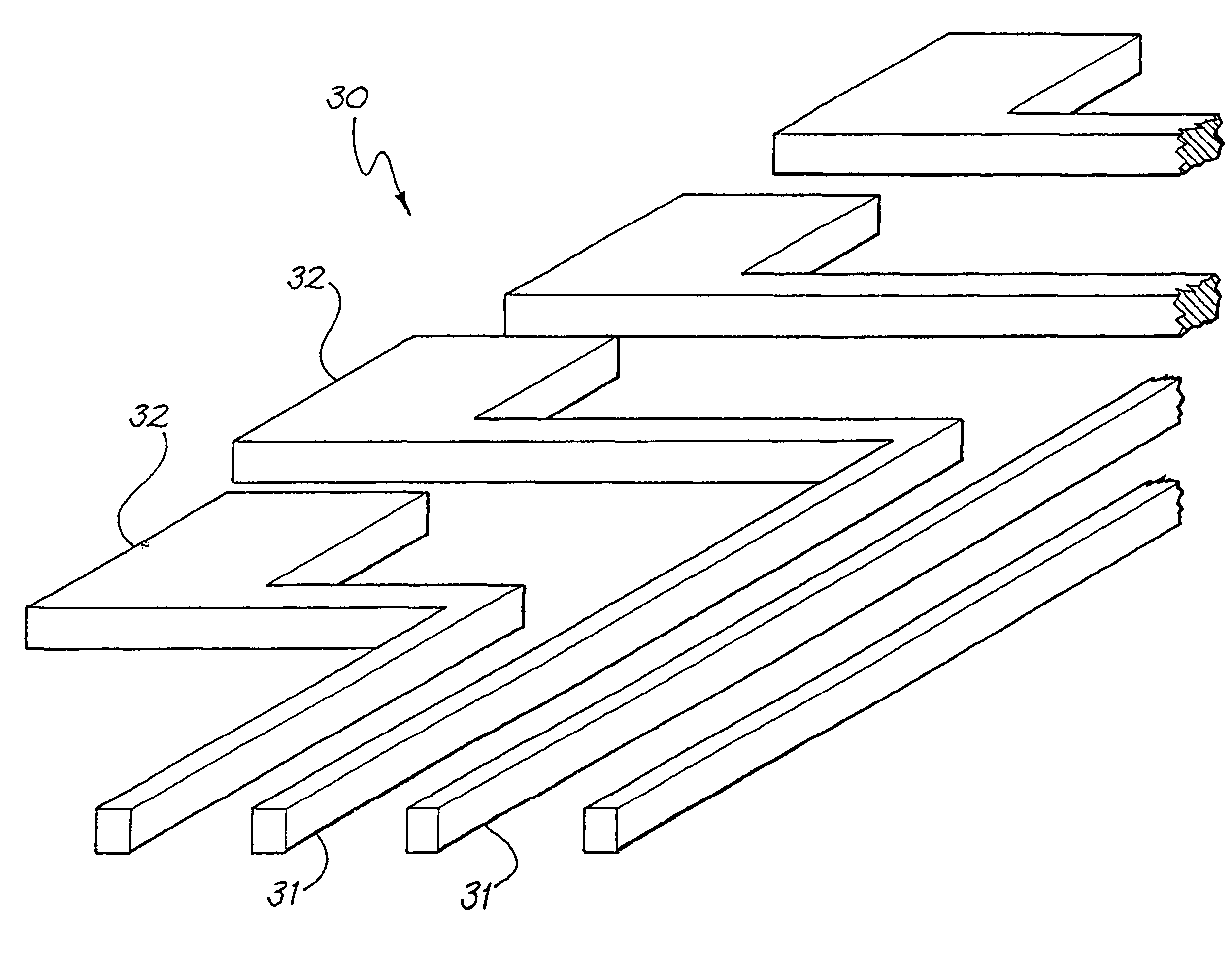
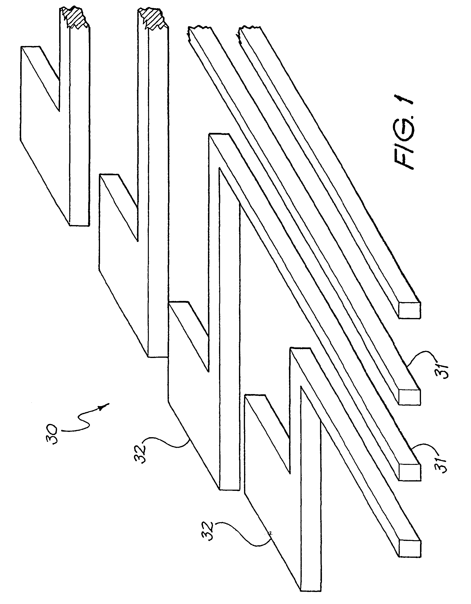
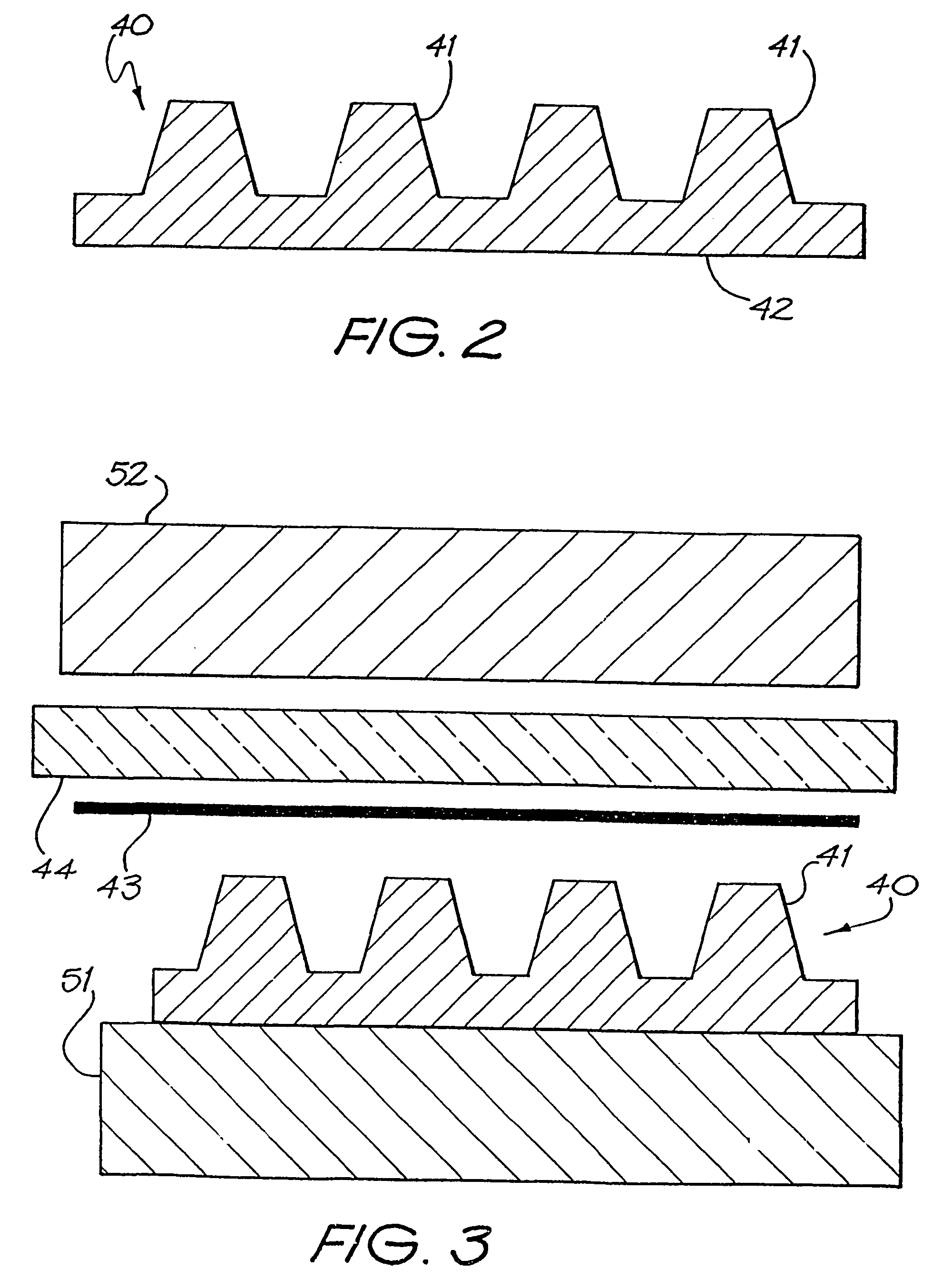
Image

Examples
Embodiment Construction
[0201]Before describing the features of the present invention, it is appropriate to briefly describe the construction of one type of known cochlear implant system with reference to FIG. 16.
[0202]Known cochlear implants typically consist of two main components, an external component including a speech processor 29, and an internal component including an implanted receiver and stimulator unit 22. The external component includes a microphone 27. The speech processor 29 is, in this illustration, constructed and arranged so that it can fit behind the outer ear 11. Alternative versions may be worn on the body. Attached to the speech processor 29 is a transmitter coil 24 that transmits electrical signals to the implanted unit 22 via a radio frequency (RF) link.
[0203]The implanted component includes a receiver coil 23 for receiving power and data from the transmitter coil 24. A cable 21 extends from the implanted receiver and stimulator unit 22 to the cochlea 12 and terminates in an electro...
PUM
| Property | Measurement | Unit |
|---|---|---|
| Thickness | aaaaa | aaaaa |
| Thickness | aaaaa | aaaaa |
| Thickness | aaaaa | aaaaa |
Abstract
Description
Claims
Application Information