
Simplified method for limiting clock pulse width

a technology of clock pulse width and simplified method, which is applied in the field of computer systems, can solve the problems of error in the interpretation of those bits, inability to synchronize the signals in the bus, and loss of charge sharing between nodes and logic values

Inactive Publication Date: 2007-07-10
GOOGLE LLC
View PDF21 Cites 2 Cited by
  • Summary
  • Abstract
  • Description
  • Claims
  • Application Information

AI Technical Summary

Benefits of technology

This approach effectively limits pulse width distortion, reduces device count, and enhances clock frequency efficiency, maintaining peak clock performance while minimizing latency and signal contamination.

Problems solved by technology

Without a precise timing mechanism, synchronizing the signals in the bus would be impossible.
One concern circuit designers have is that if the clock signal is in the ‘high’ state for too long a duration, it can discharge these pre-charged nodes or cause charge sharing between nodes and the logic value can be lost.
(In digital communications, the “eye diagram” is used to visualize how the waveforms used to send multiple bits of data can potentially lead to errors in the interpretation of those bits).
The most common causes of PWD are voltage offsets between the differential inputs and differences between the rise and fall times in the system.
PWD can be induced and coupled onto a clock signal from many different sources and is usually not uniform over all frequencies.
Excessive PWD can increase the bit error rate (BER) of a communication signal by incorrectly transmitting the data bit stream.
This leads to a violation of frequency and amplitude, causing partial or complete circuit failure.
Problems of current leakage, capacitance and signal contamination are magnified in all superscalar architectures.

Method used


Image

  • Simplified method for limiting clock pulse width
  • Simplified method for limiting clock pulse width
  • Simplified method for limiting clock pulse width

Examples


Embodiment Construction

[0028]In the following discussion, numerous specific details are set forth to provide a thorough understanding of the present invention. However, those skilled in the art will appreciate that the present invention may be practiced without such specific details. In other instances, well-known elements have been illustrated in schematic or block diagram form in order not to obscure the present invention in unnecessary detail. Additionally, for the most part, details concerning network communications, electro-magnetic signaling techniques, and the like, have been omitted inasmuch as such details are not considered necessary to obtain a complete understanding of the present invention, and are considered to be within the understanding of persons of ordinary skill in the relevant art.

[0029]In the remainder of this description, a pulse limiting circuitry (PLC) may be a sole processor of digital logical operations for correcting clock signal variations in a device. The PLC may also be one o...


PUM


Abstract

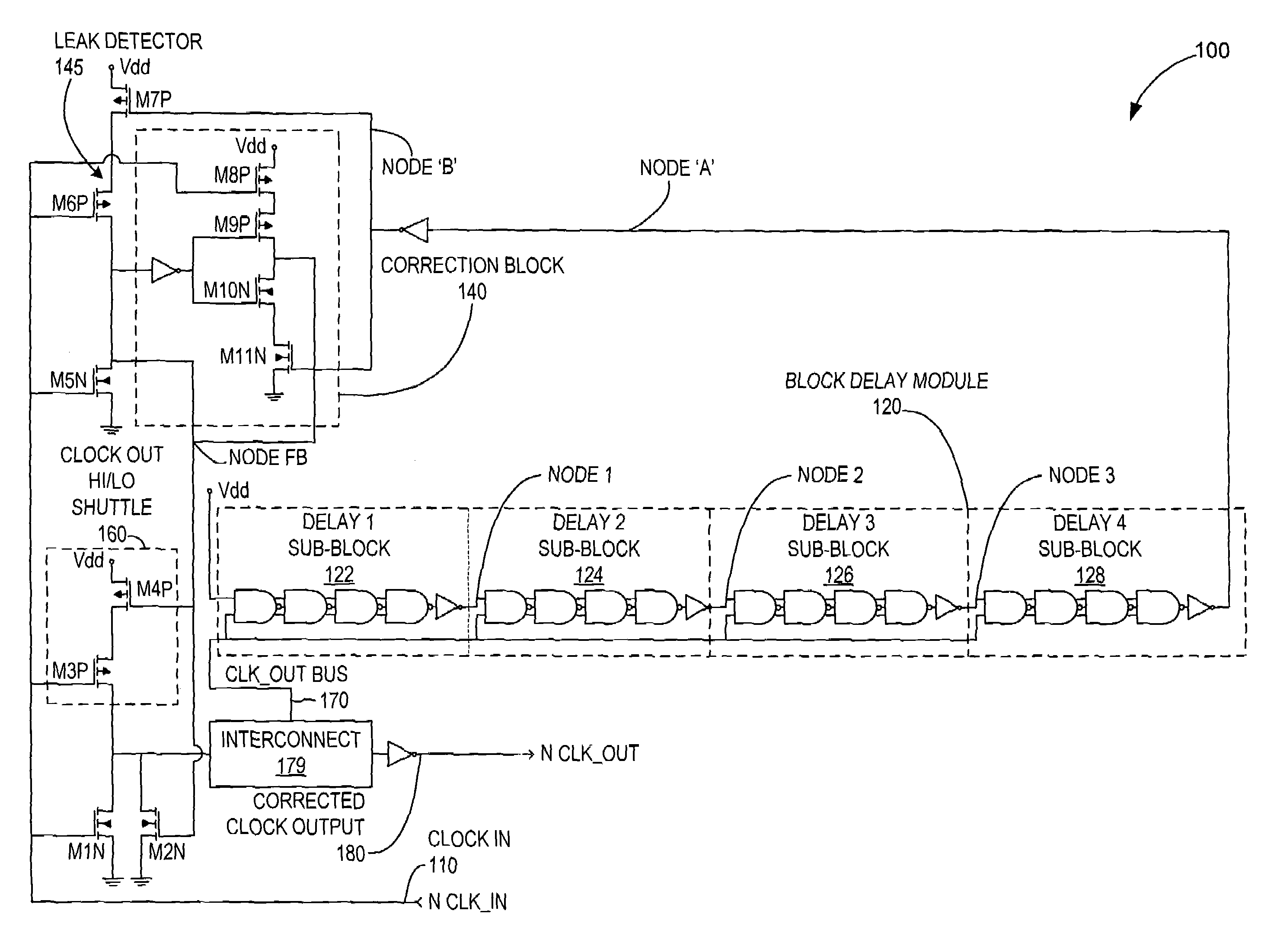
The present invention provides for correcting excessive pulse widths using incremental delays. The pulse width is evaluated through a correction block and leak detector. An acceptable pulse passes through an interconnect directly to the clock output. Unacceptable pulses are sent through a block delay module that incorporates a series of delay sub-blocks that disconnect and reset in accordance with a pre-programmed total delay time. The conditioned clock pulse is resent through a node to the correction block and leak detector where it is reevaluated. If the pulse is acceptable, it is sent to the clock output. If the pulse is found unacceptable, it is recycled again. A high low clock pulse shuttle determines and alters the high or low state of the clock pulse to ensure a correct output to downstream dependent devices.

Description

TECHNICAL FIELD[0001]The present invention relates generally to the field of computer systems and, more particularly, to limiting pulse widths in a microprocessor clock.BACKGROUND[0002]Many digital devices from the simplest gate array to the most complex circuit board can require one or more clocks, and one or more clocking signals, for a variety of routine and critical processes. An example of a critical process is the feeding of signals from a processor to a bus. Without a precise timing mechanism, synchronizing the signals in the bus would be impossible.[0003]Another example is in memory arrays where nodes are pre-charged to a specific logic level. A clock signal is applied to access these nodes or to perform some other function. One concern circuit designers have is that if the clock signal is in the ‘high’ state for too long a duration, it can discharge these pre-charged nodes or cause charge sharing between nodes and the logic value can be lost. Therefore, the goal is to limit...

Claims


Application Information

Patent Timeline
Patent Type & Authority Patents(United States)
IPC IPC(8): H03K3/017G06F1/04G06F9/45H03K5/04H03K5/156
CPCG06F1/04H03K5/04H03K5/1565
Inventor AIPPERSPACH, ANTHONY GUSBOERSTLER, DAVID WILLIAMHAILU, ESKINDER
Owner GOOGLE LLC
Learn More