On-chip receiver sensitivity test mechanism

a technology of sensitivity test and receiver, applied in the field of data communication, can solve the problems of requiring a relatively small amount of additional circuitry, and achieve the effect of reducing testing time, low cost, and high cos

Active Publication Date: 2007-08-07
TEXAS INSTR INC
View PDF8 Cites 38 Cited by
  • Summary
  • Abstract
  • Description
  • Claims
  • Application Information

AI Technical Summary

Benefits of technology

[0013]The present invention solves the problems of the prior art by providing an on-chip receiver sensitivity test mechanism for use in an integrated RF transmitter wherein the transmitter and the receiver share the same oscillator. The mechanism of the present invention obviates the need to use expensive RF test equipment with built-in modulation and BER measurement capabilities and instead permits the use of very low cost external RF test equipment to test an integrated RF receiver. A relatively small amount of additional circuitry, however, is required to realize the test mechanism on the integrated circuit. Further, this additional circuitry, software or a combination of the two would typically only be used once at the time of IC production testing to verify performance of the receiver. In most cases, the additional chip real estate taken by the test mechanism circuitry, which is not used during normal operation of the chip, is more than offset by the savings in both test time and test cost since high cost RF test equipment is not needed and testing time is reduced.
[0014]A key feature of the present invention is that it takes advantage of already existing circuitry in the transceiver in performing sensitivity testing of the receiver. In particular, the modulation circuitry and the local oscillator, normally used to generate a modulated RF carrier during transmission, is used to generate the modulated test signal that otherwise must be provided by expensive external RF test equipment having modulation capability. The modulated local oscillator signal is then mixed with an unmodulated continuous wave (CW) RF signal applied to the RF in / out terminal of the transceiver to generate a modulated IF signal which is then processed by the remainder of the receiver circuit. A consequence of modulating the oscillator already present on-chip with the test data is that the external RF test generator only need provide an unmodulated CW RF signal to the RF input terminal of the chip. This requirement can be provided by relatively low cost RF generators, thus reducing the testing costs significantly.
[0016]The modulated signal at IF is processed by the remainder of the receiver chain, wherein the signal is digitized and demodulated. The recovered Rx data bits (i.e. with bit errors) are compared by a BER meter or counter within the chip against the known test sequence used, and a BER reading is generated. The BER reading is output to an external tester which establishes a pass / fail indication for the test, or is alternatively read into an on-chip processor or controller adapted to execute a testing sequence for production testing. Once testing is complete, the processor or controller memory may be reloaded with software that would be used in the transceiver's normal operation, thus eliminating the need to allocate dedicated memory space for the testing routines.

Problems solved by technology

A relatively small amount of additional circuitry, however, is required to realize the test mechanism on the integrated circuit.
In particular, the modulation circuitry and the local oscillator, normally used to generate a modulated RF carrier during transmission, is used to generate the modulated test signal that otherwise must be provided by expensive external RF test equipment having modulation capability.

Method used


Image

  • On-chip receiver sensitivity test mechanism
  • On-chip receiver sensitivity test mechanism
  • On-chip receiver sensitivity test mechanism

Examples


Embodiment Construction

Notation Used Throughout

[0030]The following notation is used throughout this document.

[0031]

TermDefinitionASICApplication Specific Integrated CircuitBISTBuilt-in Self TestBITBuilt-in TestDCDirect CurrentDCODigitally Controlled OscillatorDPLLDigital Phase Locked LoopDSPDigital Signal ProcessorDUTDevice Under TestFCWFrequency Command WordFPGAField Programmable Gate ArrayGSMGlobal System for Mobile CommunicationHDLHardware Description LanguageIFIntermediate FrequencyISIIntersymbol InterferenceISMIndustrial Scientific MedicalMNECModulation Noise Estimation CircuitMNEMModulation Noise Estimation MechanismnDCONormalized Digitally Controlled OscillatorPCPersonal ComputerPLLPhase Locked LoopPNPseudorandom NumberRFRadio Frequency

DETAILED DESCRIPTION OF THE INVENTION

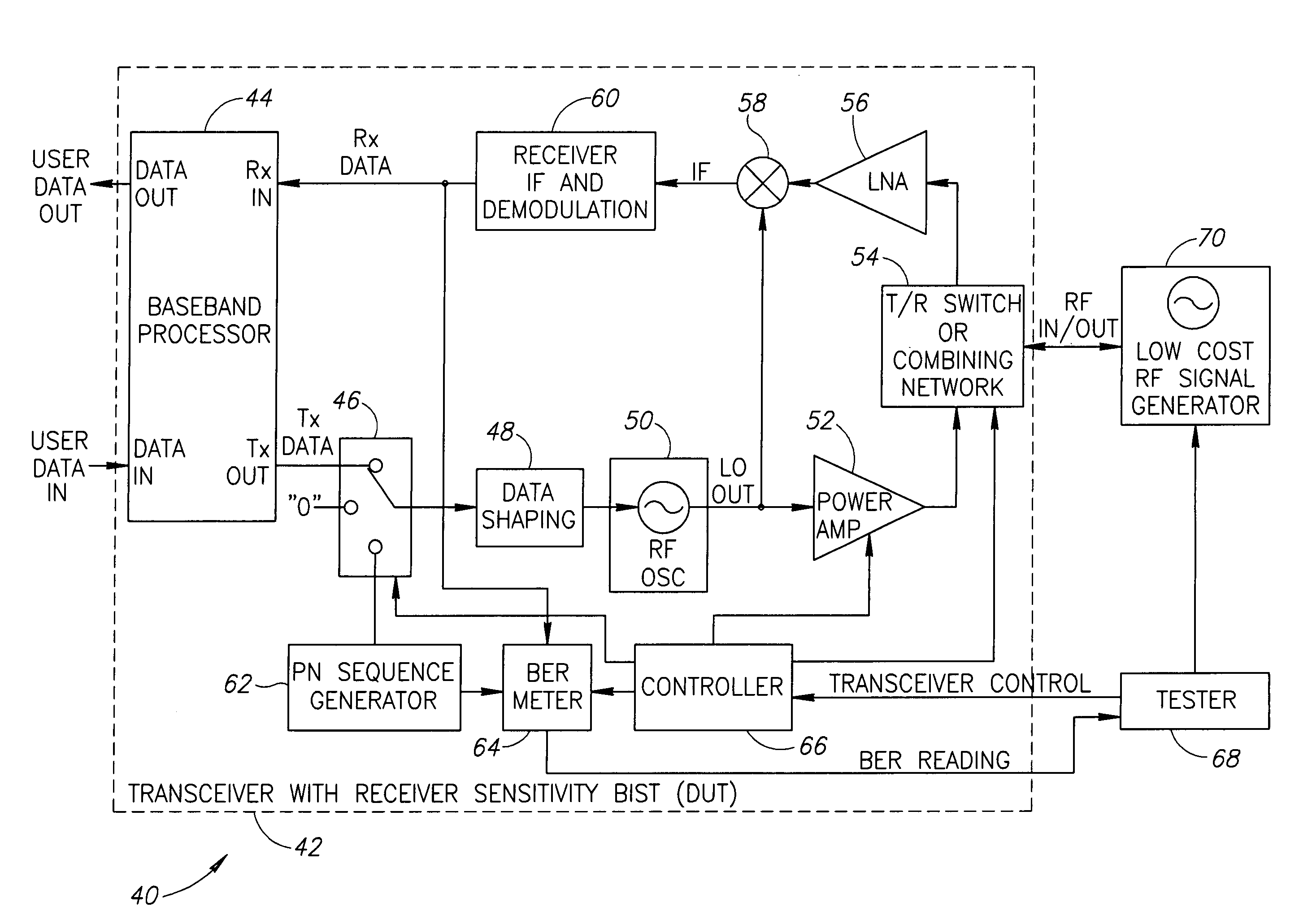
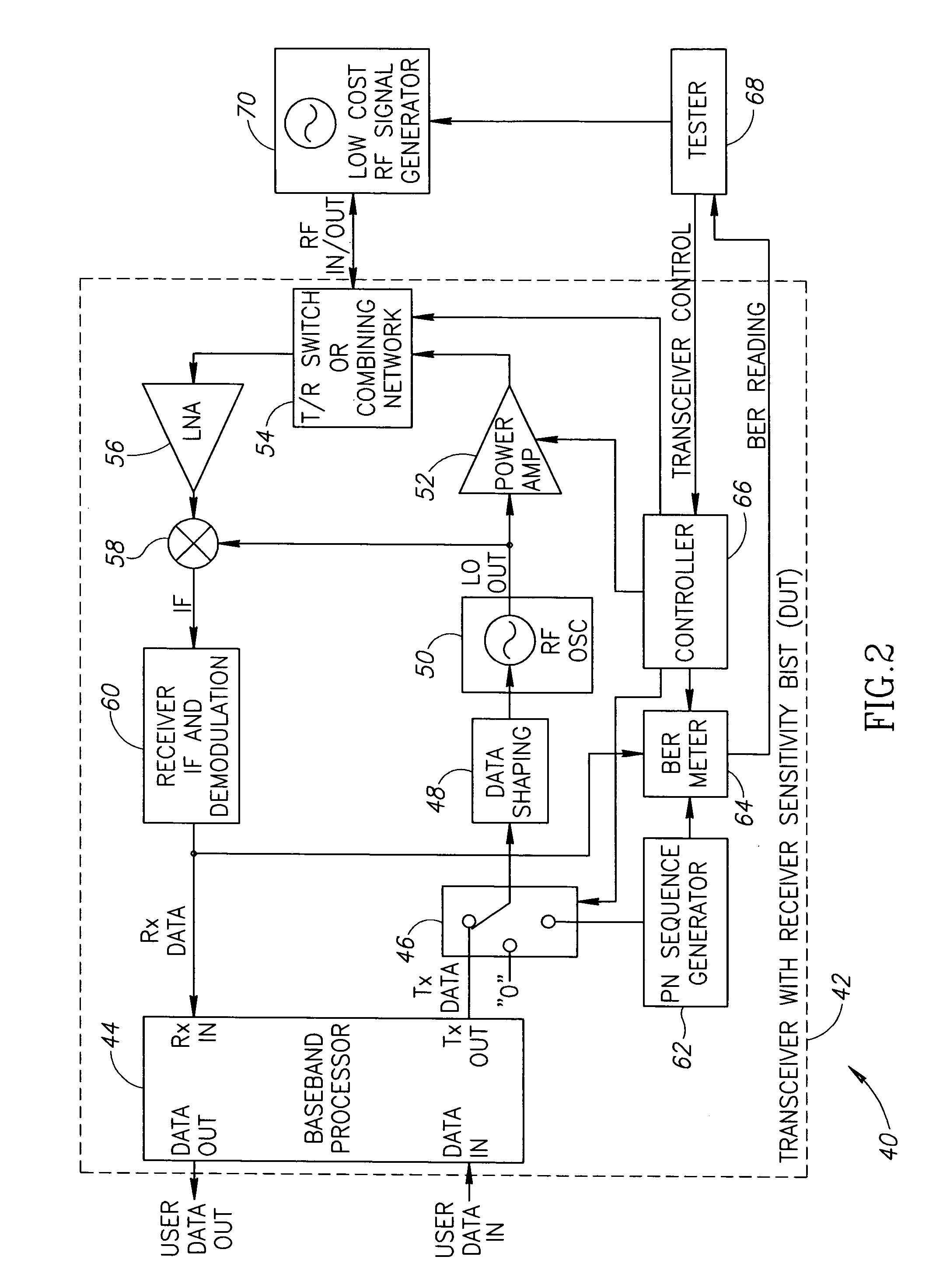
[0032]The present invention is an on-chip digital receiver test mechanism for use in an integrated RF transmitter wherein the transmitter and the receiver share the same oscillator. The mechanism of the present invention obviates ...


PUM


Abstract

An on-chip receiver sensitivity test mechanism for use in an integrated RF transmitter wherein the transmitter and the receiver share the same oscillator. The mechanism obviates the need to use expensive RF signal generator test equipment with built-in modulation capability and instead permits the use of very low cost external RF test equipment. The invention utilizes circuitry already existing in the transceiver, namely the modulation circuitry and local oscillator, to perform sensitivity testing. The on-chip LO is used to generate the modulated test signal that otherwise would need to be provided by expensive external RF test equipment with modulation capability. The modulated LO signal is mixed with an externally generated unmodulated CW RF signal to generate a modulated signal at IF which is subsequently processed by the remainder of the receiver chain. The recovered data bits are compared using an on-chip BER meter or counter and a BER reading is generated. The BER reading is used either externally or by an on-chip processor or controller to establish a pass / fail indication for the chip.

Description

REFERENCE TO RELATED APPLICATIONS[0001]This application is based on U.S. Provisional Application Ser. No. 60 / 441,080, filed Jan. 17, 2003, entitled “Type-II-All-Digital PLL in Deep-Submicron CMOS”, incorporated herein by reference in its entirety.FIELD OF THE INVENTION[0002]The present invention relates to the field of data communications and more particularly relates to an on-chip test mechanism for testing the sensitivity of a receiver suitable for use with single chip digitally implemented radio transceivers such as those constructed according to the Bluetooth or GSM standards.BACKGROUND OF THE INVENTION[0003]Designing Built-in Test (BIT) or Built-In Self Test (BIST) capabilities into semiconductor devices (i.e. chips) is a well-known technique used to place the circuitry needed to perform critical performance tests directly on the chip rather than off chip. Without the built in test circuitry, external test equipment must be used to perform the various performance tests. Several...

Claims


Application Information

Patent Timeline
Patent Type & Authority Patents(United States)
IPC IPC(8): H04B17/00G01R31/28G06F17/50H04L1/24
CPCH04B17/29H04L1/24H04B17/0085G01R31/2822
Inventor DE OBALDIA, ELIDA ISABELLEIPOLD, DIRKELIEZER, ORENKATZ, RANSTASZEWSKI, BOGDAN
Owner TEXAS INSTR INC
Why Eureka
Try Eureka