

Built-in self test for memory arrays using error correction coding
a self-testing and memory array technology, applied in the field of memory architectures with built-in self-testing capability, can solve the problems of inability to utilize or repair conditionally passed ics, inability to distinguish between tests, and failure to accept memory, so as to improve the ic manufacturing yield and reduce the test tim
- Summary
- Abstract
- Description
- Claims
- Application Information
AI Technical Summary
Benefits of technology
Problems solved by technology
Method used
Image

Examples
Embodiment Construction
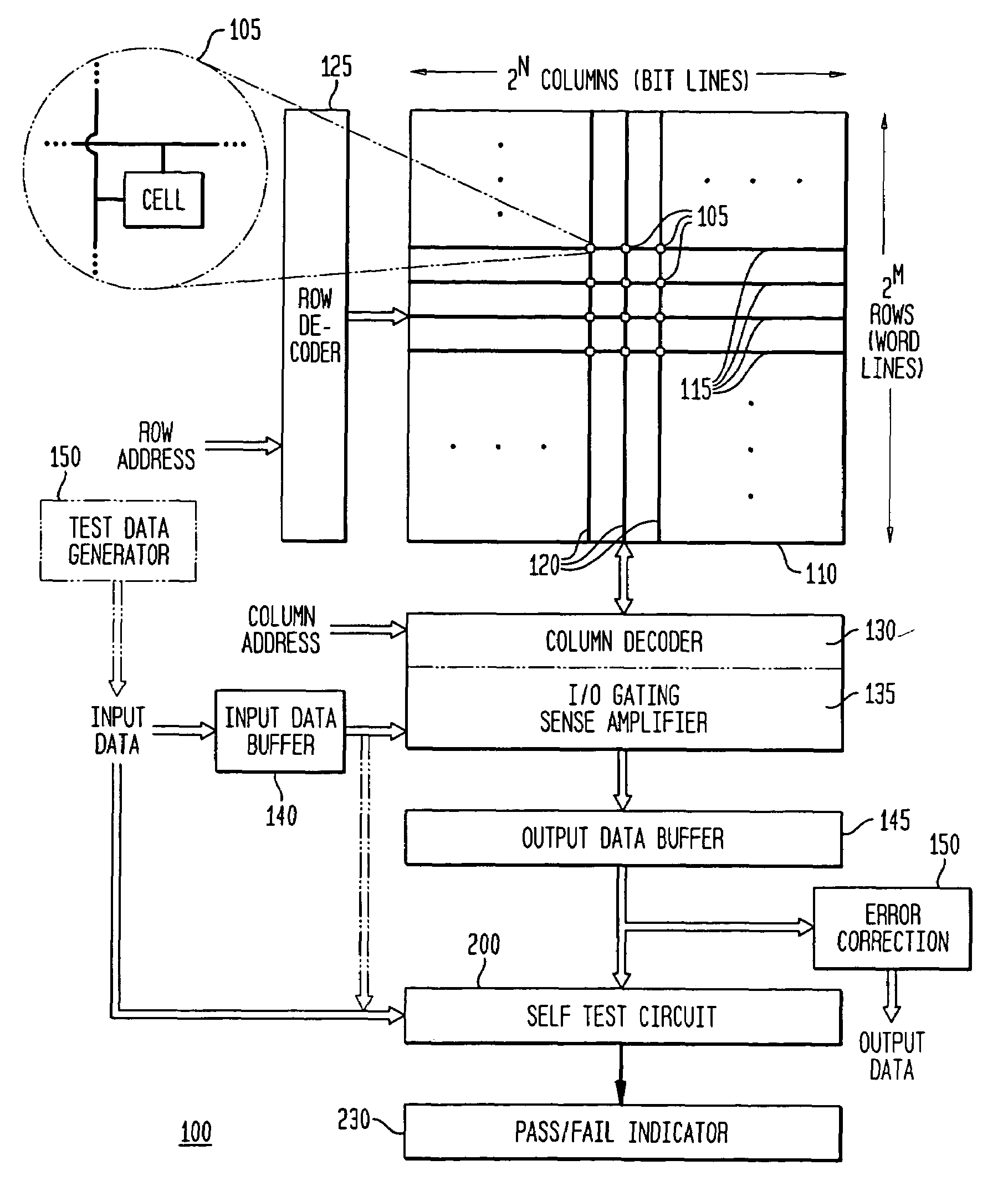
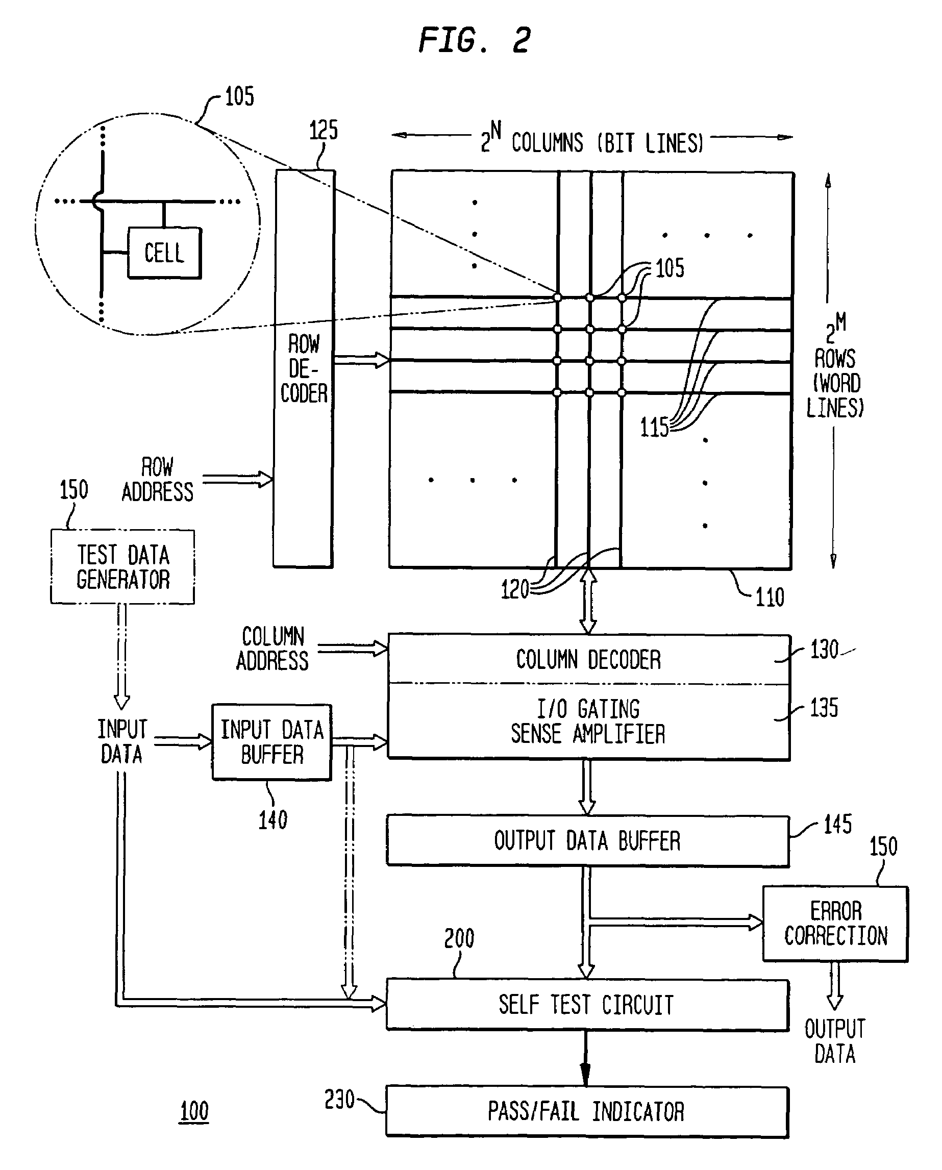
[0020]While the present invention is susceptible of embodiment in many different forms, there are shown in the drawings and will be described herein in detail specific embodiments thereof, with the understanding that the present disclosure is to be considered as an exemplification of the principles of the invention and is not intended to limit the invention to the specific embodiments illustrated.
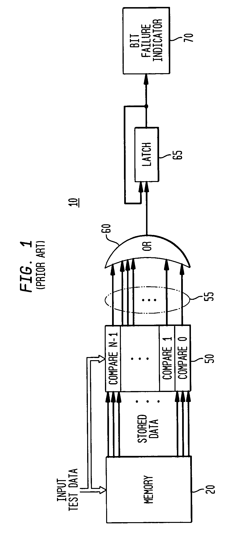
[0021]As mentioned above, the various embodiments of the present invention provide built-in self-testing (“BIST”) for a memory array which can differentiate between levels or amounts of defects or other faults. The various embodiments of the built in memory self-testing of the present invention provide for detecting bit errors, and for differentiating those memory ICs having bit errors which are correctable within the capability of a selected error correction code from those memory ICs having bit errors which are not correctable or which otherwise exceed the capability of the selected error...
PUM
 Abstract
Description
Claims
Application Information