Method for manufacturing low cost electroluminescent (EL) illuminated membrane switches

a technology of electroluminescent and membrane switches, applied in the field of membrane switches, can solve the problems of complex and bulky assemblies, unsuitable for many electronics product applications, and unsuitability of many electronics products, and achieve the effects of low cost, high production efficiency, and high production efficiency

Inactive Publication Date: 2007-08-14
NOVATECH ELECTRO LUMINESCENT
View PDF1 Cites 45 Cited by
  • Summary
  • Abstract
  • Description
  • Claims
  • Application Information

AI Technical Summary

Benefits of technology

[0014]In an exemplary embodiment of the invention, the method of the present invention includes the following steps. In the first step, a light transmissive process carrier film having metal foil bonded to its surface is prepared for further process by die cutting or chemically etching the bonded metal foil to from the desired front capacitive electrode bus, membrane switch contacts and electrical shunt, power input distribution elements and associated electrical contacts to produce a planar flexible circuit board. Following this, the basis flexible circuit board carrier film is placed onto a commercially available transport system that incorporates an optical registration system to precisely position the image area, for the remaining print and die cutting process cycles. This method allows the precise (+ / −<0.002″ in X, Y and θ axis) physical positioning of the basis carrier film without deleterious effect upon the positioning reference means. Using this positioning method allows practically unlimited numbers of print layers to be applied, and final die cutting of the completed product, without concern for layer-to-layer alignment.
[0024]The method of the present invention provides the ability to manufacture EL illuminated membrane switches at a cost fractional of that of comparable conventional construction. Additionally, these lower-cost EL illuminated membrane switches can be manufactured on readily obtainable automated production equipment. Further features and advantages of the present invention will be appreciated by a review of the following detailed description when taken in conjunction with the following drawings.

Problems solved by technology

Adding illumination to such membrane switches can create both complicated and bulky assemblies tat are unsuitable for many electronics product applications.
Additionally, these structures are also bulky, and require great care in their design and manufacture in order to make them successful for many electrical and electronic applications.
As this construction also requires individual layers to be assembled, including illuminated actuating elastomeric structures and frames, a bulky and complex assembly results.
However, this method only provides illumination during switch contact, and is also limited in the amount of electrical current the switch contacts may carry.
The use of conductive inks as switch elements also severely limits their useful life cycle.
Additionally, this method does not provide electrical circuit separation between the switch portion and the illumination circuit portion without introducing an additional switch contact and shunt set with attendant construction and isolation layers.
Thus, high voltage alternating current may add electrical interference to the switch circuit.
As the switch circuit may also make contact for voltage sensitive semiconductor devices, this lack of isolating circuits may cause both electrical interference to, and failure of such devices.

Method used


Image

  • Method for manufacturing low cost electroluminescent (EL) illuminated membrane switches
  • Method for manufacturing low cost electroluminescent (EL) illuminated membrane switches
  • Method for manufacturing low cost electroluminescent (EL) illuminated membrane switches

Examples


embodiment 100

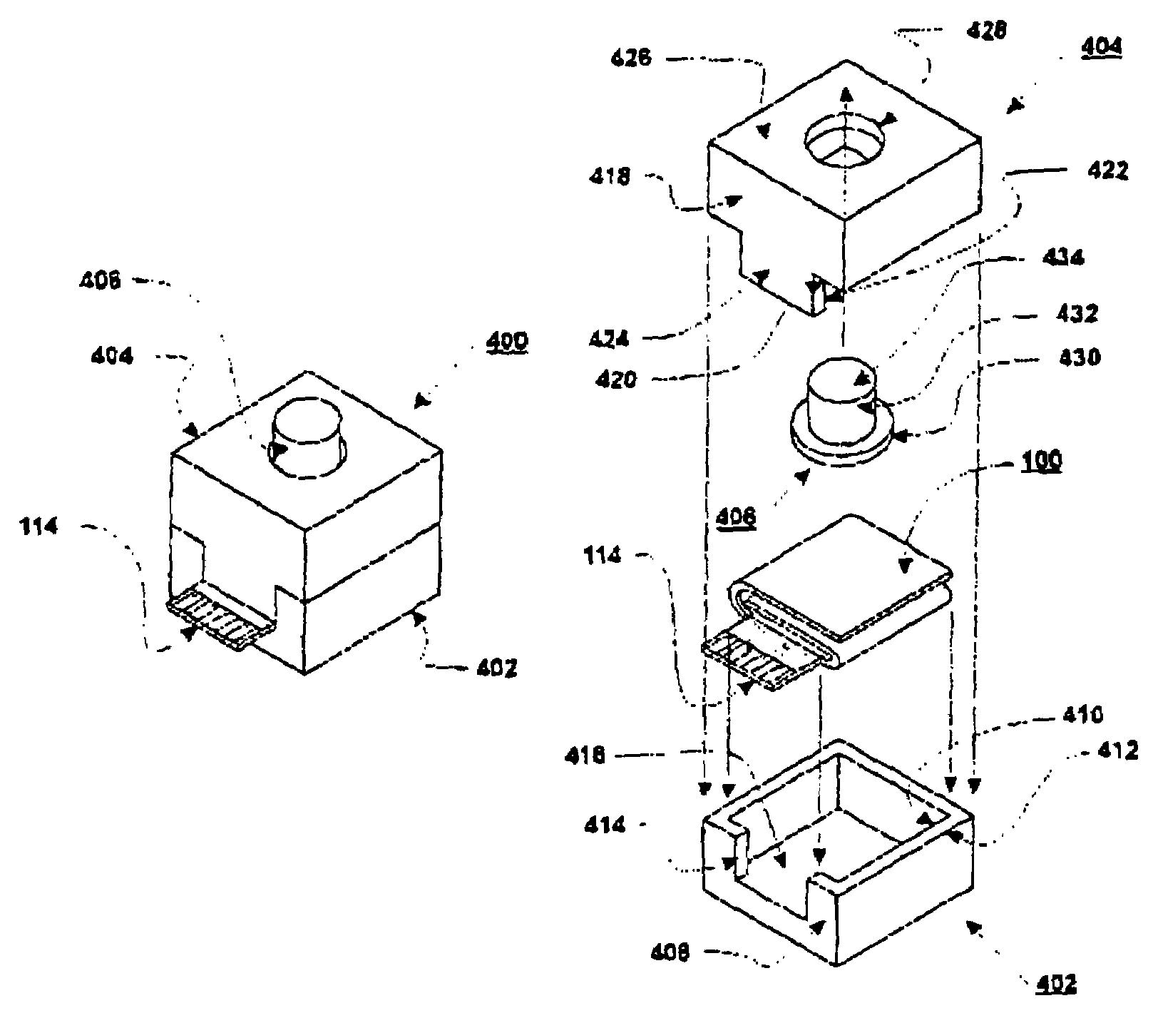
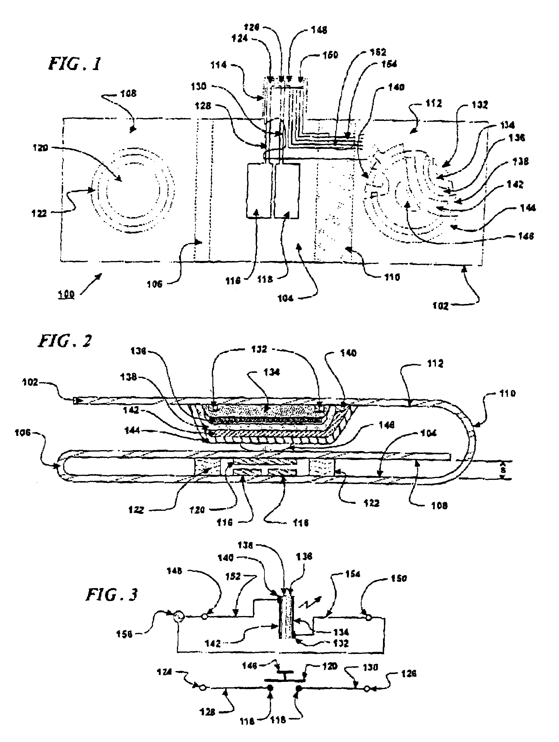
[0057]FIG. 3 provides an electrical schematic diagram of the various elements of preferred embodiment 100. When force is applied to actuator 146, shunt 120 bridges contacts 116 and 118. Electrical current path is then made beginning at terminal 124, carried by distribution path 128 to contact 116 bridging through shunt 120 to contact 118, carried by distribution path 130 to terminal 126. In a separate portion of this schematic diagram, alternating current 156 is applied to electrical terminations 148 and 150. Current flow from electrical termination 148 is carried by distribution element 152 to rear capacitive electrode power distribution bus 140, and hence to rear capacitive plate 142. Oppositional AC current 156 is applied to electrical contact 150, carried by distribution element 154 to front capacitive electrode power distribution bus 132, and thence to front capacitive plate 134. Capacitive dielectric layer 138 isolates electroluminescent phosphor 136 and, together these layers...

embodiment 200

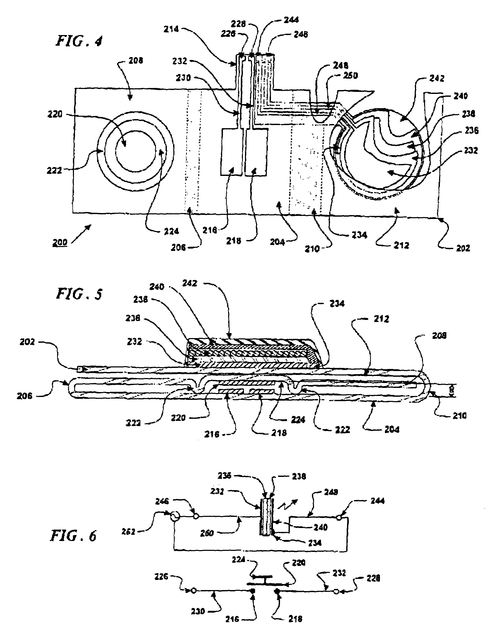
[0075]FIG. 6 provides an electrical schematic diagram of the various elements of preferred embodiment 200. When force is applied to switch actuator portion 224, shunt 220 bridges contacts 216 and 218. Electrical current path is then made beginning at terminal 226, carried by distribution path 230 to contact 216, bridging through shunt 220 to contact 218, carried by distribution path 232 to terminal 228. In a separate portion of this schematic diagram, alternating current 252 is applied to electrical terminations 244 and 246. Current flow from electrical termination 246 is carried by distribution element 250 to rear capacitive plate 232. Opposition AC current 252 is applied to electrical contact 244, carried by distribution element 248 to front capacitive electrode power distribution bus 234, and thence to light transmissive front capacitive plate 240. Capacitive dielectric layer 236 isolates electroluminescent phosphor 238, and, together these layers form a light emitting capacitor ...

embodiment 300

[0092]FIG. 9 is an electrical schematic diagram of the various elements of preferred embodiment 300. When mechanical force is applied to EL illuminated actuator plane 312, shunt 320 bridges contacts 316 and 318. Electrical current path is then made beginning at terminal 328, carried by distribution element 332 to contact 316, bridging through shunt 320 to contact 318, carried by distribution element 334 to terminal 330. In a separate portion of this schematic diagram, alternating current (AC) 356 is applied to electrical terminations 348 and 350. Current flow from electrical termination 350 is carried by distribution element 354 to rear capacitive plate 336. Oppositional AC current 356 is applied to electrical contact 348, carried by distribution element 352 to front capacitive electrode power distribution bus 338, and thence too eight transmissive front capacitive plate 344. Capacitive dielectric layer 340 isolates electroluminescent phosphor 342 and, together these layers form a l...


PUM

PropertyMeasurementUnit
thickaaaaaaaaaa
thicknessaaaaaaaaaa
flexibleaaaaaaaaaa

Abstract

A method for manufacturing low cost electroluminescent (EL) illuminated membrane switches is disclosed. The method includes the steps of die cutting, embossing or chemically etching the metal foil surface of a metal foil bonded, light transmitting flexible electrical insulation to simultaneously form one or more front capacitive electrodes, membrane switch contacts and electrical shunt, electrical distribution means and electrical terminations that together form a flexible printed circuit panel. This continuous flexible printed circuit substrate is then used with a precisely positioned indexing system.

Description

[0001]The Divisional of application Ser. No. 09 / 942,339 Filed on Aug. 30, 2001 U.S. Pat. No. 6,698,085.BACKGROUND OF THE INVENTION[0002]1. Field of the Invention[0003]The present field of the invention relates to membrane switches, and more particularly to a method for manufacturing membrane switches that are illuminated using electroluminescent lamps.[0004]2. Description of the Prior Art[0005]Present membrane switches are typically made from flexible plastic insulators that contain two layers of opposing electrically conductive surfaces isolated from one another by an air gap such that, when one surface is mechanically deformed by applied pressure, that deformed surface makes mechanical contact against the opposing stationary surface and completes an electrical current path between them. This current path may carry either signal or power electrical charge, or both. By positioning an insulating mask between these two surfaces, effective mechanical isolation ensures that unwanted ele...

Claims


Application Information

Patent Timeline
Patent Type & Authority Patents(United States)
IPC IPC(8): H01J9/00H01H11/00H01H13/83
CPCH01H13/83H01H2219/018H01H2219/037H01H2229/004H01H2229/016Y10T29/49105H01H2229/038H01H2239/01Y10T29/49156Y10T29/49155H01H2229/02
Inventor STEVENSON, WILLIAM C.LAU, JAMES
Owner NOVATECH ELECTRO LUMINESCENT
Why Eureka
Try Eureka