

Diamond triode devices with a diamond microtip emitter
a diamond triode and emitter technology, applied in the field of vacuum microelectronics, can solve the problems of unsatisfactory emission performance, unsatisfactory potential, non-uniform diamond coated silicon tips, etc., and achieve the effect of enhancing the emission performance of the structure, ideal or controllable balance of emission efficiency and durability
- Summary
- Abstract
- Description
- Claims
- Application Information
AI Technical Summary
Benefits of technology
Problems solved by technology
Method used
Image

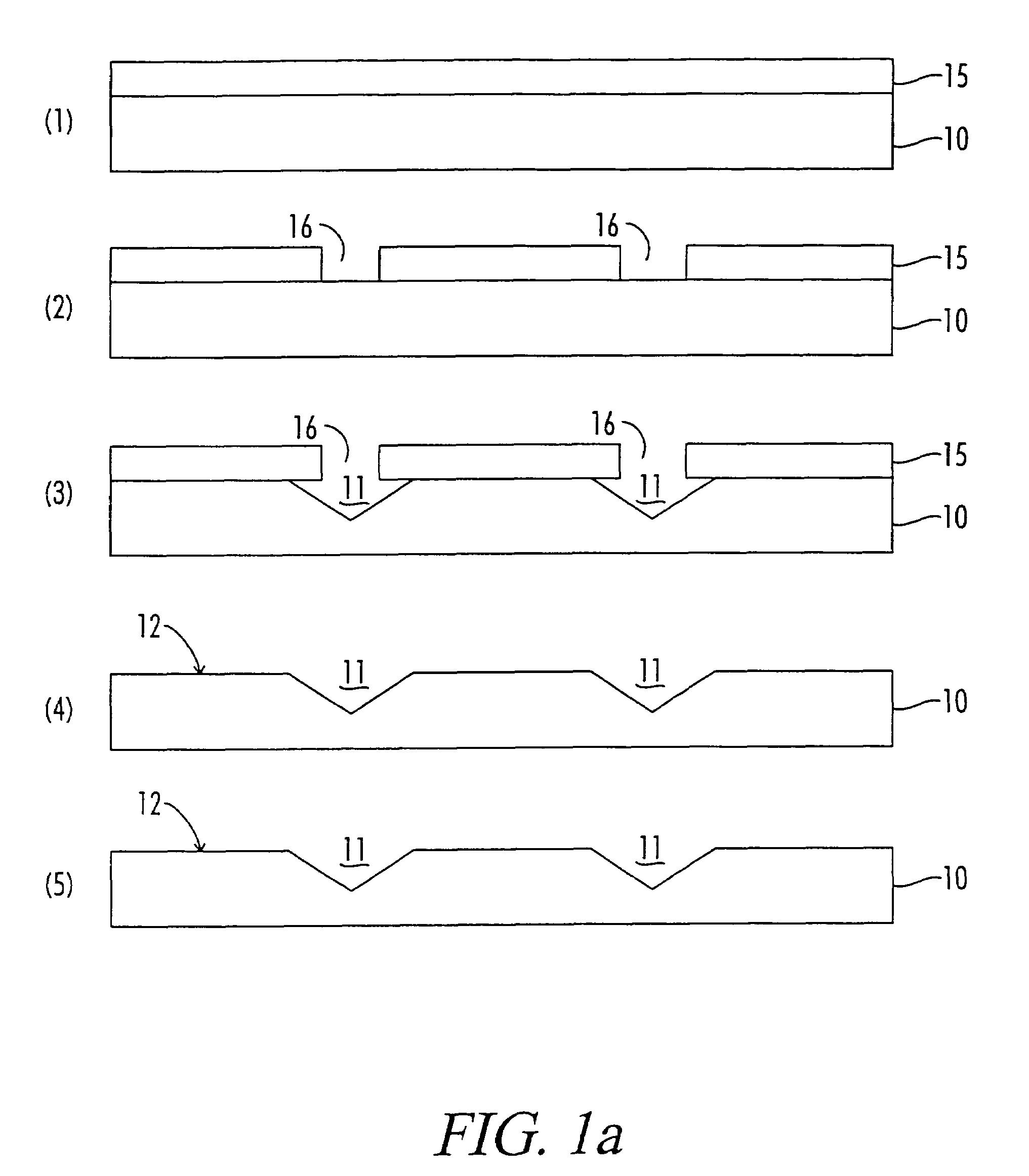
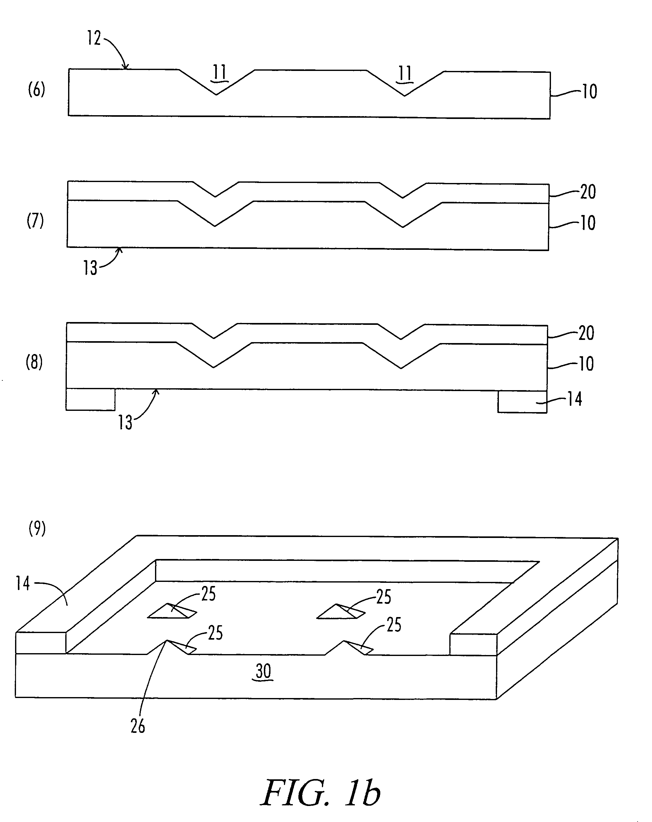
Examples
second embodiment
[0184]FIG. 26 is a diamond diode pressure sensor utilizing a conducting gate or anode 35, an insulator 40, and a pyramidal diamond microtip emitter 25 (as a cathode) on a flexible diamond substrate 30.
third embodiment
[0185]FIG. 27 shows a diamond diode pressure sensor utilizing a pyramidal diamond microtip emitter 25 on a diamond substrate 30, an insulating layer 40, and a flexible diamond diaphragm as the anode 35. In the embodiment of FIG. 27, the anode 35 will move toward or away from the emitter 25 in response to pressure changes outside the chamber 38.
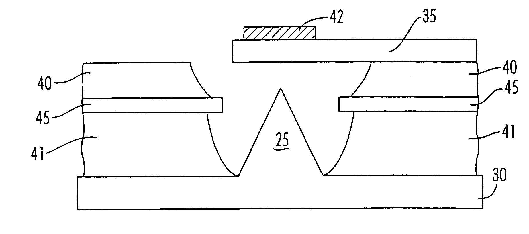
[0186]The pressure sensor of FIG. 28 uses a diamond vacuum triode device, having a diamond microtip emitter 25 on a diamond substrate 30, a grid 45 supported above the substrate 30 by a first insulating layer 41, and a flexible diaphragm (diamond, for example) as an anode 35, supported by a second insulating layer 40.
[0187]FIG. 29 illustrates an arrangement of a pyramidal diamond microtip emitter 25 as diode accelerometer device. One end of a flexible diamond substrate 30 is suspended in cantilever fashion from an insulator 40 that extends upwardly from an anode 35. If the device is subjected to a change in velocity, the substrate will flex, p...
PUM
| Property | Measurement | Unit |
|---|---|---|
| grain size | aaaaa | aaaaa |
| emission current | aaaaa | aaaaa |
| particle size | aaaaa | aaaaa |
Abstract
Description
Claims
Application Information