Method for making large scale multilayer dielectric diffraction gratings on thick substrates using reactive ion etching

a technology of reactive ion etching and dielectric diffraction grating, which is applied in the direction of optical resonator shape and construction, instrumentation, etc., can solve the problems of inability to meet the cpa requirements, the limiting factor of the power achievable with the diffraction grating system, and the prior art design and fabrication method of advanced gratings using non-metallic materials have inherently higher laser damage thresholds than prior metallic grating

Active Publication Date: 2007-08-14
GENERAL ATOMICS
View PDF14 Cites 29 Cited by
  • Summary
  • Abstract
  • Description
  • Claims
  • Application Information

AI Technical Summary

Problems solved by technology

Diffraction gratings are the limiting factor to the power achievable with these systems, since a final grating must withstand this high power density in order to reform the short pulse.
Prior art designs and fabrication methods for advanced gratings that use non-metallic materials have inherently higher laser damage threshold that prior metallic gratings.
This grating is impractical for the CPA application since the high efficiency and large chromatic bandwidth required for the CPA application means that the multilayer would have to contain many layers (>20) to have high reflectivity.
This large number of layers will act to planarize the patterned surface, destroying the grating structure.
This solution would also not be applicable due to many reasons.
The planarization layer will cause additional evanescent losses for the diffraction grating limiting the efficiency.
Also, the incident beam would have to travel through the substrate, which is not practical for short, high peak power pulses due to the potential for damage to the substrate resulting from self-focusing.
This is due to stresses in the coating or even the weight of the substrate itself being able to deform the substrate to an extent that it is unusable unless the thickness of the substrate is sufficient to prevent this distortion.
For small-size gratings in which the thickness of the substrate is inherently thin (less than 0.5 cm) and for gratings fabricated with ion-beam etching processes, the substrate thickness is not important, However, reactive ion etching has proven challenging in the fabrication of large size multilayer diffraction gratings in which the substrate is thick, e.g., at least 2.0 cm.

Method used


Image

  • Method for making large scale multilayer dielectric diffraction gratings on thick substrates using reactive ion etching
  • Method for making large scale multilayer dielectric diffraction gratings on thick substrates using reactive ion etching
  • Method for making large scale multilayer dielectric diffraction gratings on thick substrates using reactive ion etching

Examples


Embodiment Construction

[0023]The following description is not to be taken in a limiting sense, but is made merely for the purpose of describing the general principles of exemplary and preferred embodiments.

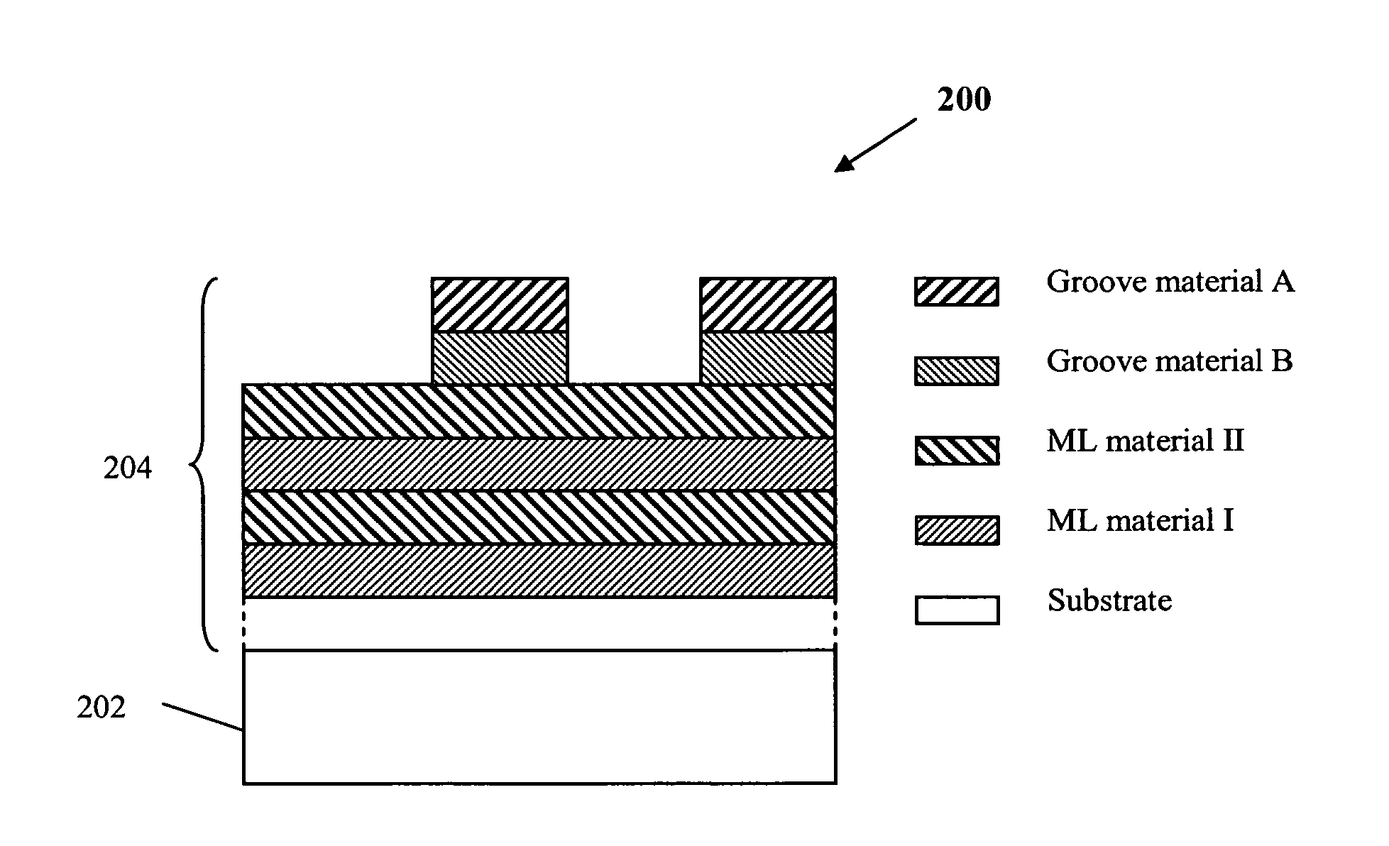
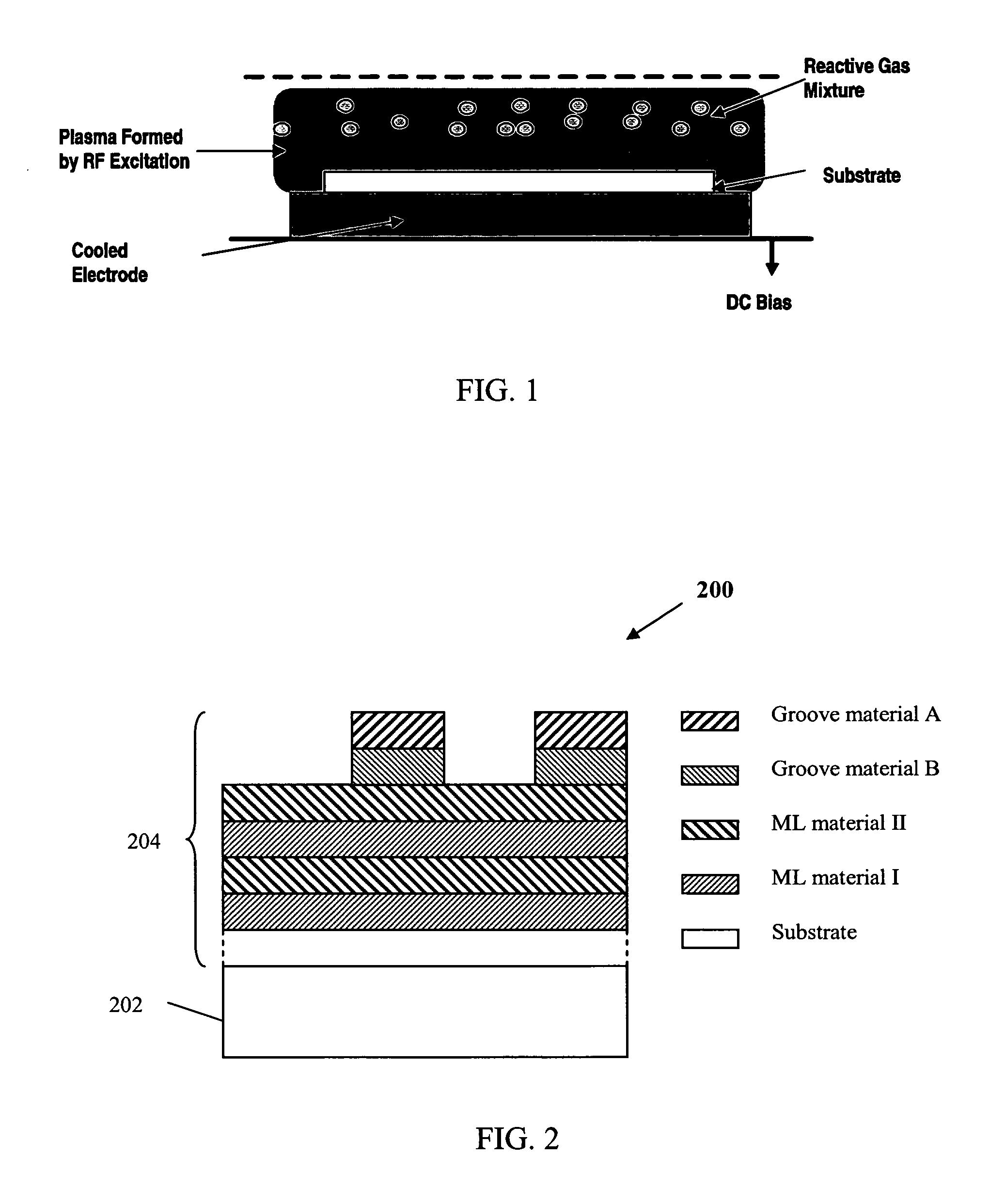
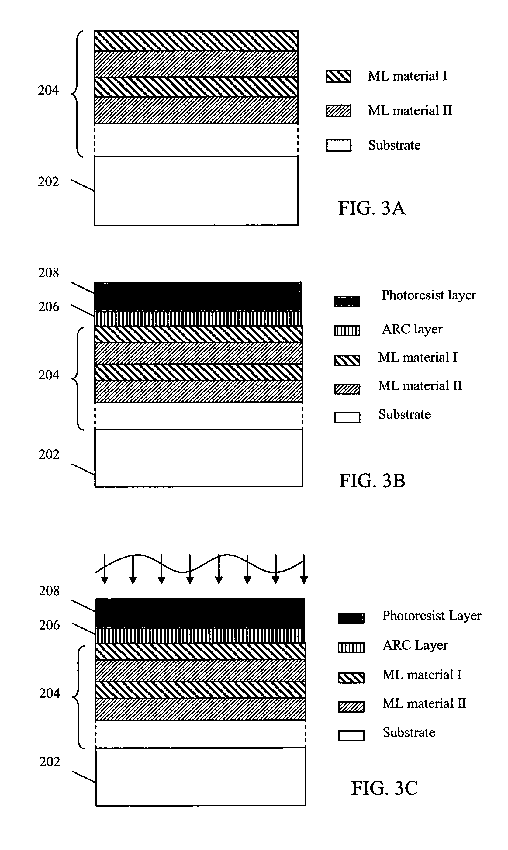
[0024]Referring first to FIG. 2, a diagram is shown of a large multilayer diffraction grating formed with a thick substrate in accordance with one embodiment of the invention. The multilayer diffraction grating 200 includes a substrate 202 having a multilayer dielectric structure 204 formed thereon. The multilayer dielectric structure 204 includes several layers of dielectric material, for example, having alternating indexes of refraction and is also referred to as a dielectric stack. For example, illustrated are multilayer (ML) material I and multilayer (ML) material II. It is understood that the multilayer structure 204 may have any number of desired layers (as illustrated by dashed lines extending from the dielectric structure 204 to the substrate 202). Furthermore, the top layer / s of the multilayer ...


PUM


Abstract

Methods of fabricating large size, high performance multilayer diffraction gratings having a thick substrate that take advantage of reactive ion etching during the fabrication process are provided herein. In one implementation, a method of making a multilayer diffraction grating comprises the steps of: providing a substrate having a thickness of at least 2.0 cm; applying a dielectric structure having a plurality of layers on the substrate; depositing a photoresist; exposing the photoresist to a grating pattern; developing the photoresist to produce the grating pattern in the photoresist; and reactive ion etching to transfer the grating pattern to the dielectric structure. In preferred form, the substrate material of the grating is selected to have low electrical resistivity and high thermal conductivity.

Description

[0001]This application claims the benefit of U.S. Provisional Application No. 60 / 554,224, filed Mar. 17, 2004, which is incorporated herein by reference.BACKGROUND OF THE INVENTION[0002]1. Field of the Invention[0003]The present invention relates generally to diffraction gratings, and more specifically to the manufacture of multilayer diffraction gratings.[0004]2. Discussion of the Related Art[0005]Diffraction gratings are integral parts of chirped-pulse amplification (CPA) high peak power lasers. In this scheme, high peak power is achieved by creating a laser pulse which contains an energy density near the saturation fluence of the laser medium and a duration near the inverse of its gain narrowed bandwidth. Diffraction gratings are used to distribute the energy of the laser pulse over a much longer time period prior to amplification in order to prevent damage to the laser amplifier. Following amplification, the pulse is compressed to extremely high power density by passage through ...

Claims


Application Information

Patent Timeline
Patent Type & Authority Patents(United States)
IPC IPC(8): G02B5/18G02B27/44
CPCG02B5/1857
Inventor BARTON, IAN MICHAELPERRY, MICHAEL DALE
Owner GENERAL ATOMICS
Why Eureka
Try Eureka