Unlock instant, AI-driven research and patent intelligence for your innovation.

Method and apparatus for an efficient memory built-in self test architecture for high performance microprocessors

a self-testing, high-performance microprocessor technology, applied in the direction of measurement devices, error detection/correction, instruments, etc., can solve the problems of reduced width of test buses, reduced diagnostic efforts, and reduced test bus overhead

Active Publication Date: 2007-08-21
ORACLE INT CORP
View PDF44 Cites 23 Cited by
  • Summary
  • Abstract
  • Description
  • Claims
  • Application Information

AI Technical Summary

Benefits of technology

[0012]In accordance with the invention, a memory BIST architecture is disclosed which provides an efficient communication interface between external agents, e.g., external tester, and a memory BIST architecture. The memory BIST architecture reduces diagnostics efforts by dividing the search space and allowing the test and debug to be concentrated on the failing memory. The memory BIST architecture is divided into two levels, a memory BIST sequencer level and a satellite memory BIST module. The memory BIST sequencer level includes a set of registers that provide an interface between external agents attempting to communicate with the MBIST module and the satellite MBIST module.

Problems solved by technology

One challenge associated with embedded memories relates to identifying defects within the embedded memory.
Testing via a memory tester has known drawbacks including the wiring overhead of the test bus to access the memory under test and the cost of memory testers.
Thus, the test bus is reduced in width; however, the delay for serial-to-parallel conversion becomes a bottle neck for at speed memory test.
Considering complexity of these devices and the fact that the Input / Output (I / O) connections are much slower than their core clock rate, the external tester method is often an ineffective and inefficient method to test the memories embedded within large scale integrated circuits such as microprocessors.
The FSM based memory BIST controller is efficient but lacks the flexibility necessary to accommodate changes in a memory test algorithm.
However, depending on the size of the integrated circuit in which the memory BIST is embedded and the number of the memories that are tested via the memory BIST and because it is desirable for the memory BIST module to be placed close to the memories under test, the cost associated with creating this communication interface for each instantiation of a memory BIST module in a design with high number of embedded memories is high.

Method used


Image

  • Method and apparatus for an efficient memory built-in self test architecture for high performance microprocessors
  • Method and apparatus for an efficient memory built-in self test architecture for high performance microprocessors
  • Method and apparatus for an efficient memory built-in self test architecture for high performance microprocessors

Examples


Embodiment Construction

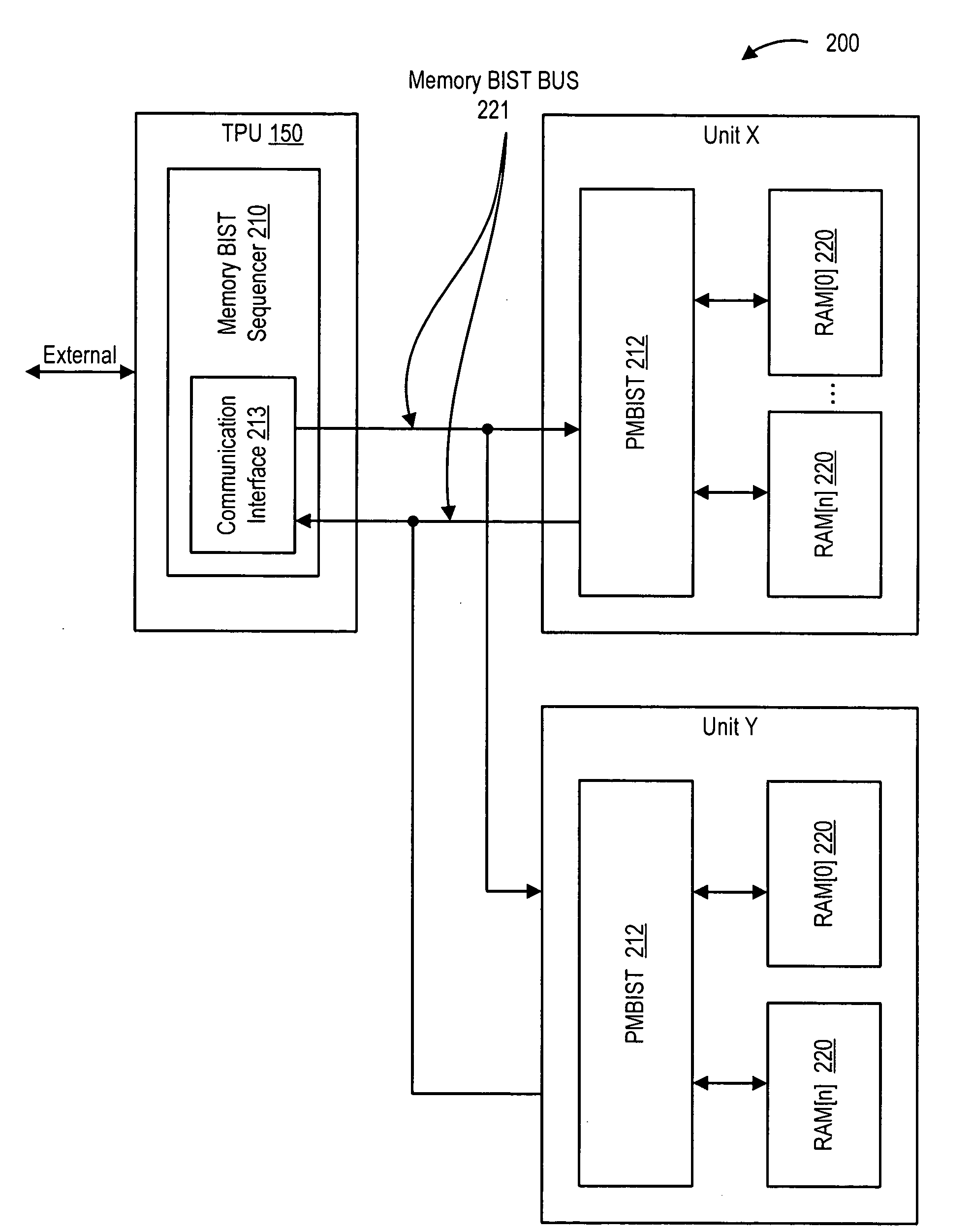
[0026]FIG. 1 shows a schematic block diagram of a multithreaded processor architecture. More specifically, processor 100 includes an instruction fetch unit (IFU) 110, an instruction renaming unit (IRU) 112, an instruction scheduling unit (ISU) 114, a floating point and graphics unit (FGU) 120, an integer execution unit (IEU) 122, a memory management unit (MMU) 130, a data cache unit (DCU) 132, a secondary cache unit (SCU) 140, an external interface unit (EIU) 142. The processor also includes a test processing unit (TPU) 150 and a performance hardware unit (PHU) 152.

[0027]The instruction fetch unit 110 includes an instruction cache and branch prediction logic. The instruction fetch unit 110 is coupled to the instruction renaming unit as well as to the memory management unit 130 and the secondary cache unit 140.

[0028]The instruction renaming unit is coupled to the instruction fetch unit 110 and to the instruction scheduling unit 114. The instruction renaming unit 112 includes dependen...


PUM


Abstract

A memory BIST architecture provides an efficient communication interface between external agents, e.g., external tester and a memory BIST module. The memory BIST architecture reduces diagnostics efforts by dividing the search space and allowing the test and debug to be concentrated on the failing memory. The memory BIST architecture is divided into two levels, a memory BIST sequencer level and a satellite memory BIST module. The memory BIST sequencer level includes a set of registers that provide an interface between external agents attempting to communicate with the MBIST module and the Satellite MBIST module.

Description

BACKGROUND OF THE INVENTION[0001]1. Field of the Invention[0002]The present invention relates to processors having embedded memories and more particularly to exposing and debugging defects within embedded memories of processors.[0003]2. Description of the Related Art[0004]Digital systems include data paths, control paths and memories. Many known digital systems, such as microprocessors, include embedded memories. One challenge associated with embedded memories relates to identifying defects within the embedded memory. Defects in memories may be due to shorts and opens in memory cells of the embedded memories, address decoder(s) and read / write logic. These defects may be modeled as Stuck-at Faults (SAF), Transition Faults (TF), Stuck Open Faults (SOF), Address Decoder Faults (AF), Coupling Faults (CF) and Neighborhood Pattern Sensitive Faults (NPSF) in the memory cells.[0005]Pluralities of classes of test algorithms have been proposed for detection of the memory faults. The pluraliti...

Claims


Application Information

Patent Timeline
Patent Type & Authority Patents(United States)
IPC IPC(8): G01R31/28
CPCG01R31/3187
Inventor ZARRINEH, KAMRANHOUSE, KENNETH A.OBAIDULLA, SYED A.
Owner ORACLE INT CORP
Features
  • R&D
  • Intellectual Property
  • Life Sciences
  • Materials
  • Tech Scout
  • Unparalleled Data Quality
  • Higher Quality Content
  • 60% Fewer Hallucinations
Learn More