An important issue in the fabrication of such glass devices, as well as of devices which comprise one glass substrate and one other substrate, the latter being e.g. a
silicon or a
polymer substrate, as well as of devices which comprise any combination of these substrate materials, is the sealing of the microfluidic capillary circuit that is formed by combining the two substrates, of which at least one contains an etched or by other means engraved
channel pattern.
Some sealing methods use dispensed
polymer forming liquids, such as epoxies and the such as, which are considered undesirable for fluidic
chip sealing purposes for several reasons, the most important being the difficulties in dispensing a uniformly thick material layer on exact positions along the periphery of an engraved channel, the
porosity and
mechanical integrity of the material, and the interference of the material with e.g. organic solvents in the channel of the fluidic
system during operation.
Drawback is the high electrical field that is required for the process, which in some cases will result in bonding of channel walls in unwanted locations.2.
Anodic bonding of a glass to a
silicon substrate, for example as described in U.S. Pat. No. 3,397,278.
Drawback of this method is that it can only be applied for bonding of a glass substrate to a
metal or semiconducting substrate, which limits the use of the resulting devices to applications at low electrical fields and relatively low temperatures.
This method generally works well for electronic applications, but may lead to unwanted leakage in fluidic applications, in particular if the
chip is used at high pressures, which is relevant for separation and synthetic
chemistry applications.4. Thermal glass-to-glass bonding, which consists in heating both substrates to a temperature at which melting starts to occur, or at least to a temperature at which the glass starts to soften, e.g. at 550° C., and pressing the substrates together, by which a bond is formed.
This was described in the previously mentioned publication by Harrison et al., and has as important drawbacks the occurrence of leakage when one of the substrates contains surface
topography such as
metal patterns and the possible deformation of the substrates when they are pressed together in a softened or partially
molten state, by which the
structural integrity of the fluidic circuit contained in one or both of the substrates will be affected.5. Bonding of two glass substrates through an intermediate layer of a low-melting-point material, or through an intermediate layer which solidifies from a solution during heat treatment.
Drawback of this method is that the layer during dispension or during melting may destroy the
structural integrity of the fluidic circuit, due to re-flow of the material.
Consequently, the previous methods have the disadvantages that an
electric field is required for bonding, that a (partially)
molten state or application of pressure is required, and / or that the method is limited to a particular choice of substrate material or
film material on the substrate.
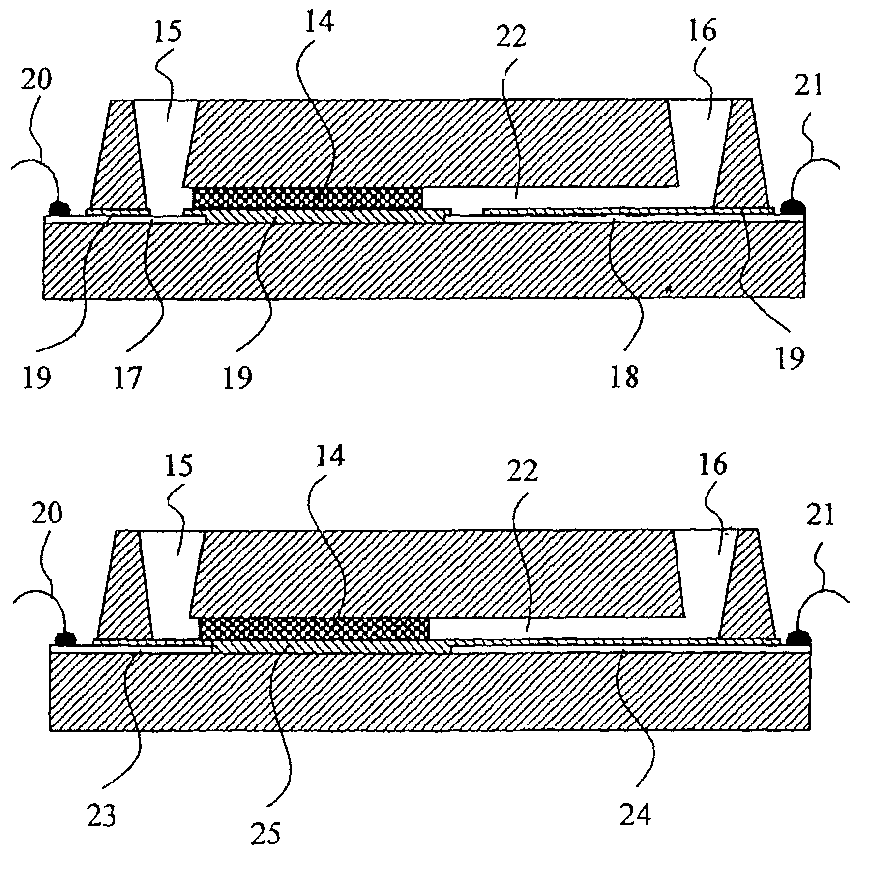
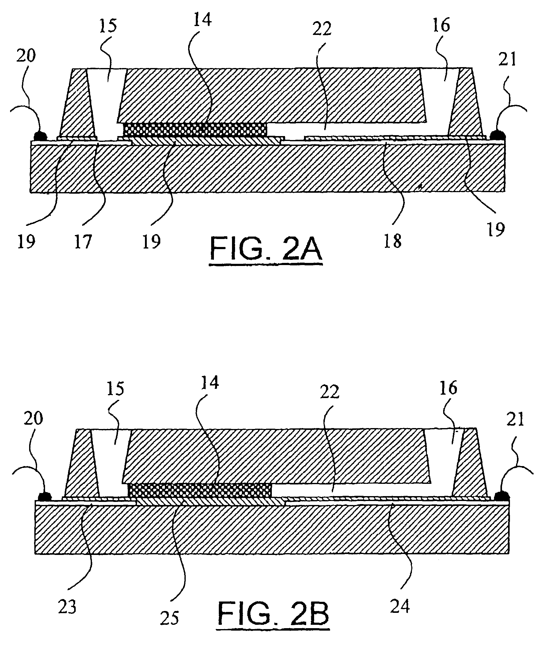
Further drawbacks of the above methods become evident from the following when sealing is required on
metal patterns that are present in-between the two glass plates, between a glass plate and a
silicon plate, or between two silicon plates.
As discussed by Harrison et al. in the previously mentioned publication, sealing over
platinum lines that extended over one of the glass substrates showed liquid leakage even after a careful heat treatment during the
thermal bonding procedure.
The prevention of leakage is crucial for fluidic microsystems, since leakage will give rise to cross-talk between adjacent fluidic conduits and leads to dead-volumes that give rise to cross-
contamination of subsequent sample injections.
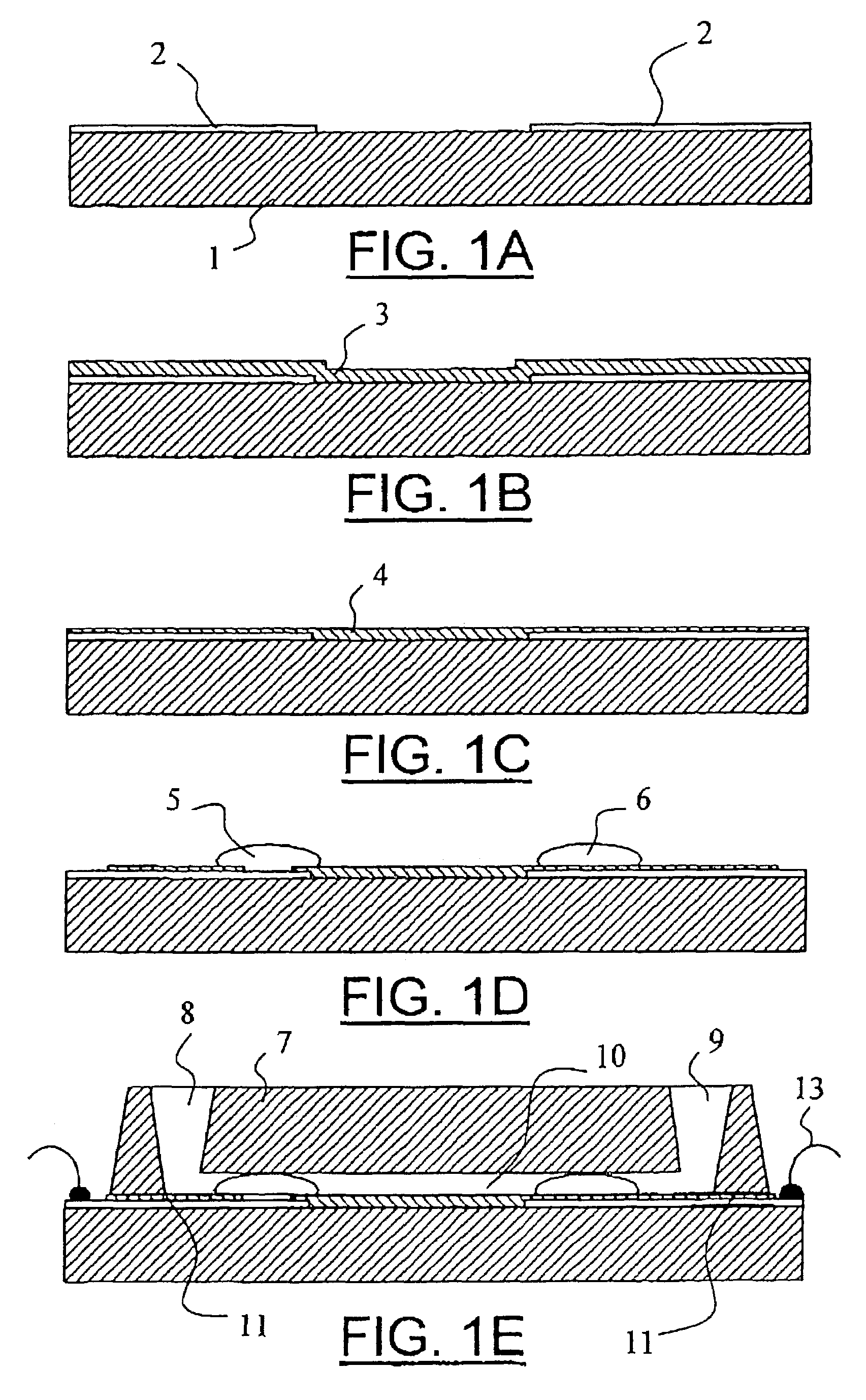
This known device is considered undesirable not only because of the extra photolithographic steps that are required during fabrication of the device, but even more because of the necessity of an exact dimensional match and positional alignment of the metal pattern with the etched recess.
In particular, the required recess depth uniformity and metal film thickness uniformity over the substrate area, as well as the lithographic
overlay quality, is difficult to obtain with most state-of-the-art
etching and deposition apparatus, and can only be achieved with very well-tuned and expensive equipment.
This is the reason why the method is frequently observed to fail in conventional fabrication environments, and leak-tight sealing is not obtained with the method.

