Method for Cu metallization of highly reliable dual damascene structures

a damascene and high-reliability technology, applied in the direction of semiconductor devices, semiconductor/solid-state device details, electrical equipment, etc., can solve the problems of ashing, resist removal, and special challenges for fabricating damascene structures made of copper inlay and low-k ild materials that cannot be corrected by cmp processing, and achieves the effect of avoiding voids, avoiding voids, and avoiding voids

Inactive Publication Date: 2007-08-28
SONY CORP +1
View PDF22 Cites 25 Cited by
  • Summary
  • Abstract
  • Description
  • Claims
  • Application Information

AI Technical Summary

Benefits of technology

[0010]It is an object of the present invention to provide improved processes for fabrication of damascene structures. Another object is to provide damascene structures free of surface defects in the manufacture of integrated circuits.

Problems solved by technology

However, there exist special challenges for fabricating damascene structures made of copper inlay and low-k ILD materials that cannot be corrected by CMP processing.
Surface irregularities and other topography issues such as dishing or erosion created during the etching, ashing, resist removal, and cleaning steps are potentially more damaging in dual-damascene than in non-damascene processes.
However, the resulting damascene structure exhibits failure (e.g. voids) at the surface interface between the copper feature 32 and the dielectric layer 20.
Such defects in the surface result in electromigration resistance within the structure and pose performance and reliability issues in the finished devices.

Method used


Image

  • Method for Cu metallization of highly reliable dual damascene structures
  • Method for Cu metallization of highly reliable dual damascene structures

Examples


Embodiment Construction

[0015]A more complete understanding of the method and apparatus of the present invention is available by reference to the following detailed description of the embodiments when taken in conjunction with the accompanying drawings. The detailed description of the embodiments which follows is intended to illustrate but not limit the invention. The scope of the invention is defined by the appended claims.

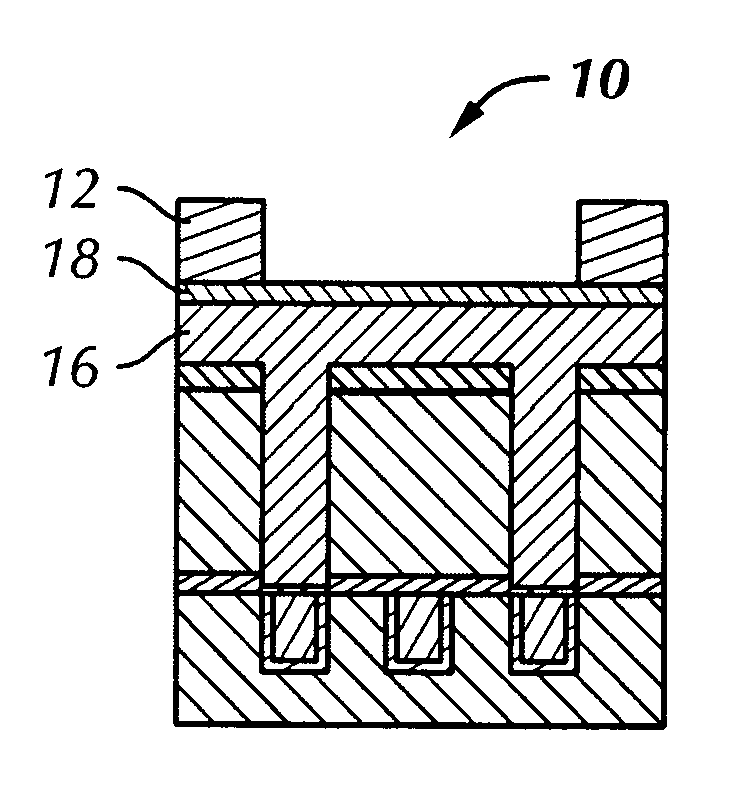
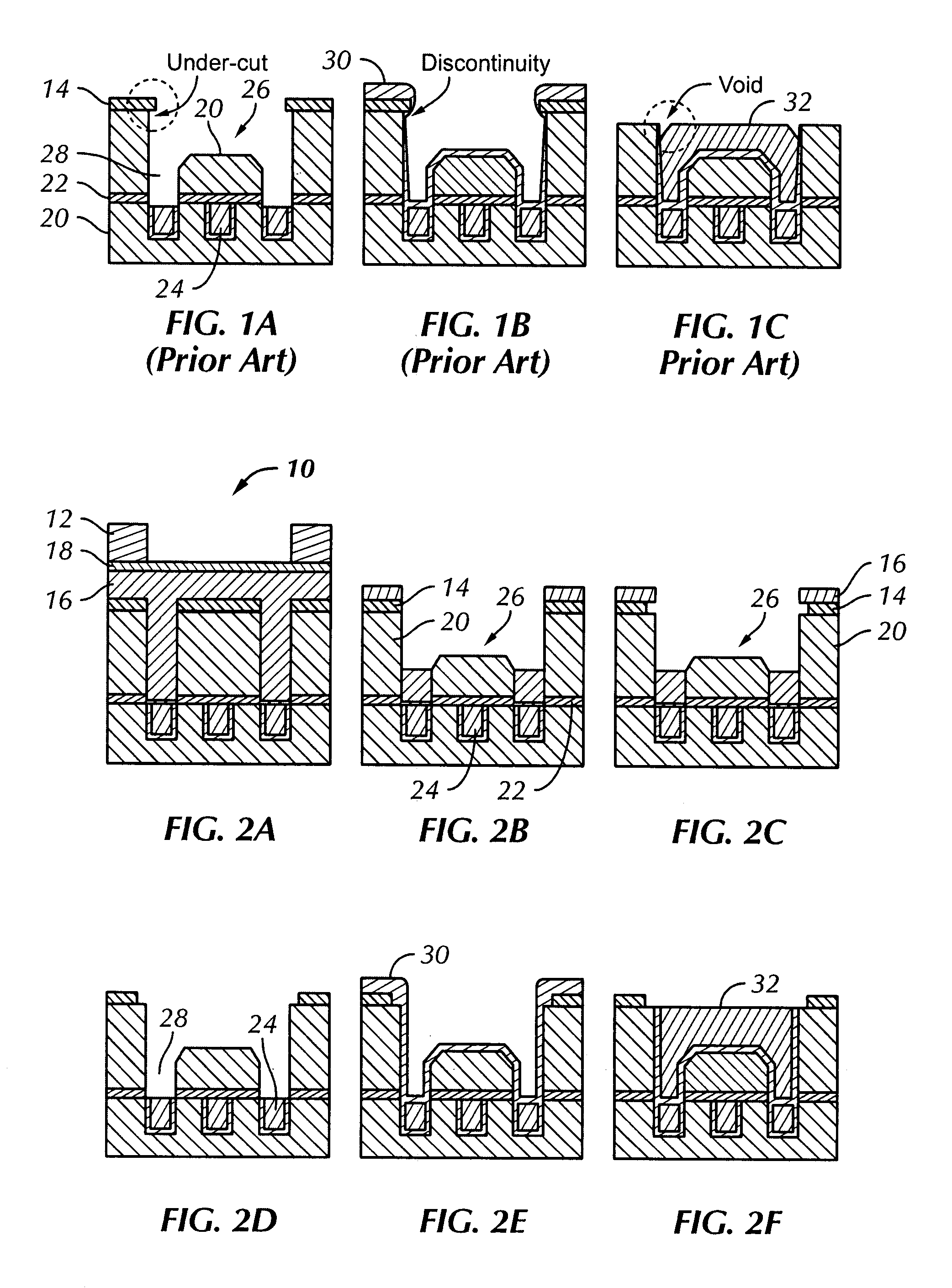
[0016]The present invention provides a method for forming a void-free copper damascene structure from a composite comprising a substrate having a conductive structure, a first dielectric layer on the substrate, a diffusion barrier layer on the first dielectric layer, and a second dielectric layer on the barrier layer. The method comprises forming a via opening by etching the second dielectric layer, the diffusion barrier layer and the first dielectric layer to expose the conductive structure by developing a photoresist through a first hard mask which defines a via opening. The via openi...


PUM

PropertyMeasurementUnit
dielectric constantaaaaaaaaaa
conductiveaaaaaaaaaa

Abstract

The present invention provides a method for forming a void-free copper damascene structure comprising a substrate having a conductive structure, a first dielectric layer on the substrate, a diffusion barrier layer on the first dielectric layer, and a second dielectric layer on the barrier layer. The method comprises forming via and trench openings developing a photoresist through a first and second hard mask. The first hard mask is laterally etched such that it is eroded to a greater extent from the trench opening with respect to the underlying second dielectric layer. Remaining gap fill layer is removed and the diffusion barrier layer within the via opening is etched to expose the conductive structure. The via and trench openings are plated with a barrier metal and a copper seed layer to obtain copper features that fill the openings and form a void-free copper damascene structure.

Description

FIELD OF THE INVENTION[0001]The present invention relates generally to the field of integrated circuit devices, and more particularly, to methods for fabricating void-free dual damascene structures using a copper barrier / seed.BACKGROUND[0002]As CMOS transistor scaling proceeds into the deep sub-micron regime, the signal integration of many active elements has necessitated that many layers of high density metal interconnect. To reduce device resistance and capacitance (“RC”), the industry has moved away from aluminum interconnect metal with silicon dioxide dielectric between the metal lines to copper coupled with low-K interlayer dielectric (“ILD”) materials in single and dual damascene structures. Copper metallization combined with low dielectric constant (“low-k”) ILDs has resulted in the reduction of RC time constant delays in interconnect devices. This integration of copper with low-k materials is considered to be critical to the development of next-generation ultra-large-scale i...

Claims


Application Information

Patent Timeline
Patent Type & Authority Patents(United States)
IPC IPC(8): H01L21/76H01L21/22H01L21/44H01L21/4763H01L29/40
CPCH01L21/76808H01L21/7681
Inventor ISHIKAWA, YOSHIMITSU
Owner SONY CORP
Why Eureka
Try Eureka