Light emitting device and manufacturing method of the same

a technology of light emitting devices and manufacturing methods, which is applied in the direction of electroluminescent light sources, identification means, instruments, etc., can solve the problems of reducing the number of wirings which come across the sealed portion, and affecting the reliability of light emitting elements. , to achieve the effect of enhancing the reliability of light emitting elements, and reducing the number of wirings

Inactive Publication Date: 2007-09-18
SEMICON ENERGY LAB CO LTD
View PDF19 Cites 24 Cited by
  • Summary
  • Abstract
  • Description
  • Claims
  • Application Information

AI Technical Summary

Benefits of technology

[0025]According to the invention, moisture and oxygen can be blocked from outside by a barrier film, which contributes greatly to enhance the reliability of light emitting elements. Also, by utilizing the region beside the wiring connected portion which tended to be the dead space conventionally, a frame region of a light emitting device can be narrowed, leading to the downsizing of the device, thus it can suitably be applied to a mobile terminal. Further, by disposing a signal processing circuit outside a barrier film, the number of wirings which come across the sealed portion can be reduced. Therefore, the amount of moisture and oxygen which come in from the boundary between the wirings and the barrier film can be reduced, which can further enhance the reliability.

Problems solved by technology

When forming a circuit externally, it becomes difficult to achieve the downsizing and thinner shape of a display panel since a wiring such as an FPC (Flexible Printed Circuit) for connecting the circuit to a substrate over which a pixel portion is formed is required as well as the mounting of the circuit.
It had been difficult to integrally form a signal line driver circuit, a signal processing circuit, and the like on the same substrate with a pixel portion by using conventional TFTs (Thin Film Transistors) formed of amorphous silicon since it has low mobility.
However, as for a display panel for a mobile terminal, it is supposed to undergo a difficult condition as compared to a stationary display panel regarding the case of the outside use in wet weather, danger of a drop, and the like.
However, the light emitting element is easily deteriorated by moisture, oxygen, and the like as its light emitting layer comprises an organic material or an organic material partially including an inorganic material, which may generate a dark spot or shrink.
However, even by adopting such a method, the reliability which is required for the downsized and thinner display panel has not yet been secured enough so far.

Method used


Image

  • Light emitting device and manufacturing method of the same
  • Light emitting device and manufacturing method of the same
  • Light emitting device and manufacturing method of the same

Examples


embodiment 1

[0050]FIG. 7 shows an audio signal processing circuit as an example of the signal processing circuit according to the invention. Shown here is a connection between a D / A converter circuit and a speaker-driving terminals. The audio signal processing circuit includes a D / A converter circuit 1001, a D / A converter buffer circuit 1002, a preamplifier 1003, a non-inverting amplifier for driving speaker 1004, an inverting amplifier for driving speaker 1005, speaker-driving terminals 1006 and 1007, a coupling capacitors 1009 and 1010, smoothing capacitors 1031, 1032, 1033, and 1034, a preamplifier feedback resistor 1016, gain setting resistors for driving speaker 1017 to 1020, a power supply for D / A converter circuit 1021, an analog-to-digital switch 1023, and an analog signal input terminal 1024.

[0051]The operation thereof is described now. A parallel digital audio signal is converted to an analog signal in the D / A converter circuit 1001, and then input to the analog-to-digital switch 1023...

embodiment 2

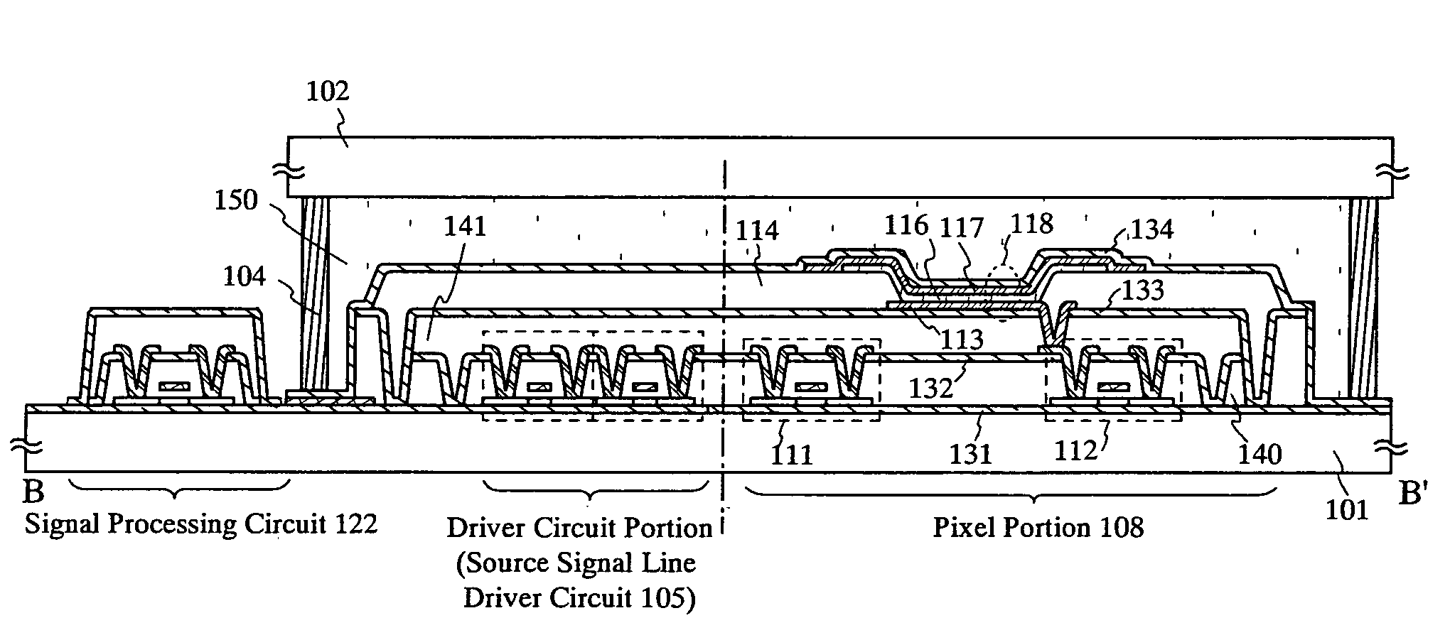
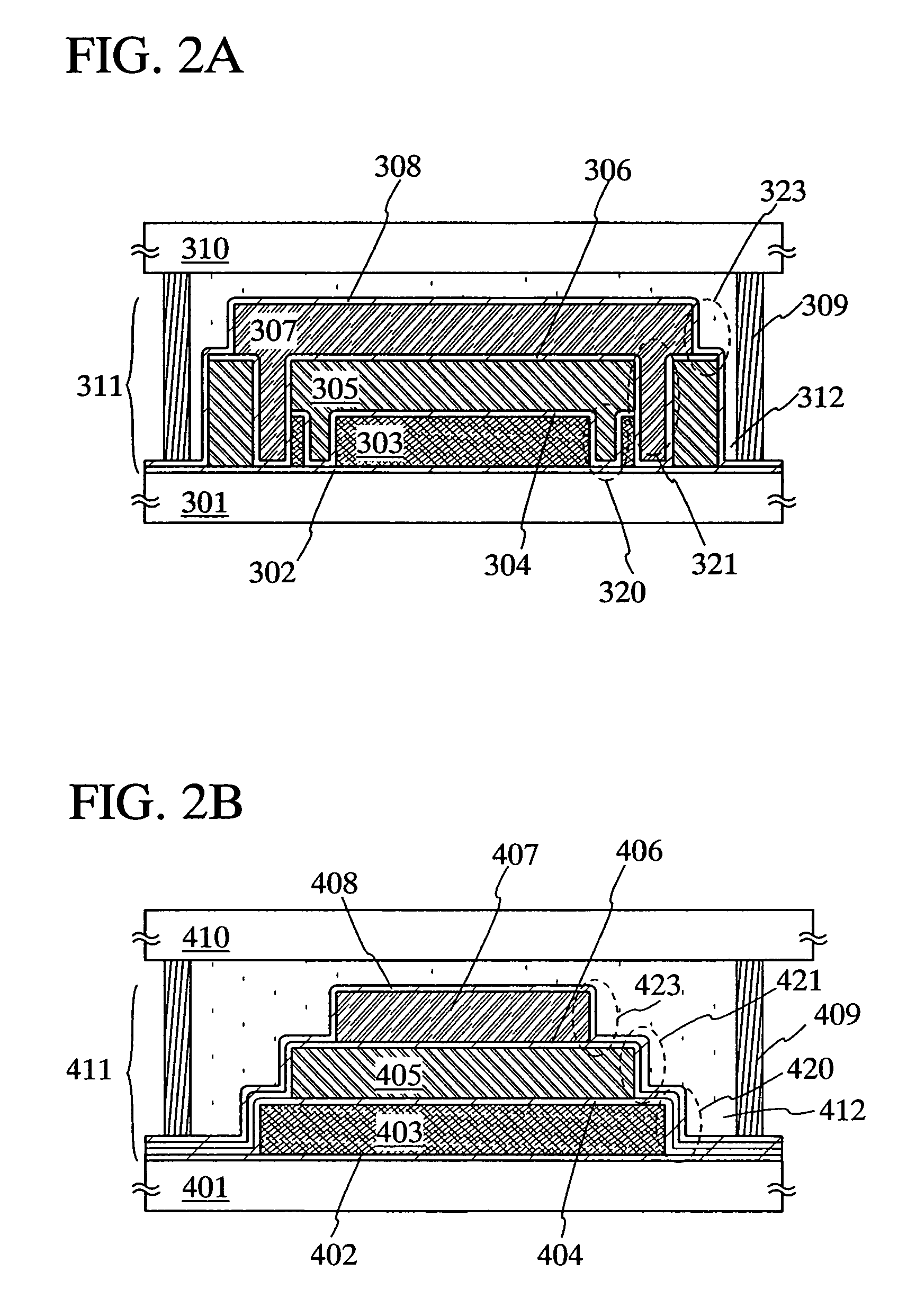
[0053]An embodiment of the invention is described now with reference to FIG. 2. FIGS. 2A and 2B each show a sealed structure of a light emitting device according to the invention.

[0054]In FIG. 2A, a first barrier film 302 is deposited over a substrate 301. The first barrier film 302 may include one or more of a silicon nitride film, a silicon nitride oxide film, and a nitrogen containing carbon film, and be formed to have a thickness of 50 nm to 500 nm by sputtering, CVD, and the like.

[0055]On the first barrier film 302, a TFT forming layer 303 in which a plurality of TFTs (Thin Film Transistors) are covered with an interlayer insulating film is formed. It is to be noted that TFT herein defined is any TFT formed by known methods and having known structures, therefore, the invention is not limited to a specific TFT. A part of the TFT forming layer 303 is formed with a first opening 320 that penetrates the TFT forming layer 303. The TFT forming layer 303 and the first opening 320 (inc...

embodiment 3

[0087]Described in this embodiment are a structure and a manufacturing method of a sealed portion with reference to FIGS. 8A and 8B.

[0088]FIG. 8A shows a preferred embodiment in the case where the structure shown in FIG. 2A is applied in Embodiment 2.

[0089]In FIG. 8A, a first barrier film 802 is deposited on a substrate 801. In this embodiment, a silicon nitride film is formed to have a thickness of 100 nm by sputtering.

[0090]Then, a TFT 803 is formed on the first barrier film 802. It is to be noted that the TFT 803 at least comprises impurity regions (source region and drain region), a channel forming region, a gate insulating film, and a gate electrode. A TFT forming layer 811 includes a plurality of TFTs. The TFT 803 shown in FIG. 8A denotes a TFT which is electrically connected to a first electrode of a light emitting element to be formed later (also referred to as a current controlling TFT). Then, a first interlayer insulating film 815 is deposited so as to cover the TFT 803. I...


PUM


Abstract

The invention provides a downsized structure of a light emitting device, and a light emitting device which has enough reliability as a downsized light emitting device. The light emitting device comprising light emitting elements according to the invention includes a signal processing circuit disposed beside an FPC and the like that tended to be the dead space conventionally. Also, the light emitting device has a sealed structure using a barrier film in which moisture and oxygen can be blocked from outside not to come into TFTs, wirings, and the light emitting elements formed over a substrate.

Description

BACKGROUND OF THE INVENTION[0001]1. Field of the Invention[0002]The present invention relates to a light emitting device comprising light emitting elements each including a pair of electrodes and a light emitting layer sandwiched between them, and a manufacturing method of the same. More particularly, the invention relates to a circuit configuration and a sealed structure of the light emitting device.[0003]2. Description of the Related Art[0004]In recent years, display panels using light emitting elements are actively developed. A light emitting element comprises a pair of electrodes (anode and cathode) and a light emitting layer sandwiched between them. The light emitting layer emits light when a voltage is applied to both electrodes. Since a display panel using the light emitting elements emits light in its light emitting layer sandwiched between both electrodes, further downsizing and thinner shape of the display panel are expected to be achieved.[0005]As an obstruction to the do...

Claims


Application Information

Patent Timeline
Patent Type & Authority Patents(United States)
IPC IPC(8): H01L29/04H05B33/04G09F9/00G09F9/30H01L27/32H01L31/20H01L51/50H01L51/52H01L51/56H05B33/14
CPCH01L27/3244H01L27/3258H01L27/1248H01L27/124H01L51/5253H10K59/12H10K59/124H10K50/844
Inventor KOYAMA, JUNMIYAKE, HIROYUKI
Owner SEMICON ENERGY LAB CO LTD
Why Eureka
Try Eureka