Liquid crystal panel

a technology of liquid crystal panels and control films, which is applied in the field can solve the problems of limit the thinning of conventional liquid crystal panels, and difficult to form alignment control films on flat substrates with curved surfaces. achieve the effects of improving the outer surface, reducing the weight of liquid crystal panels, and increasing the freedom of appearan

Active Publication Date: 2007-10-09
MERCK PATENT GMBH
View PDF21 Cites 10 Cited by
  • Summary
  • Abstract
  • Description
  • Claims
  • Application Information

AI Technical Summary

Benefits of technology

[0012]According to this aspect of invention, a liquid crystal panel having freedom in the appearance, light device weight, simplified structures, etc. is obtained by improving the outer and / or inner surfaces of the device.
[0019]By the present invention, it is possible to obtain a liquid crystal panel having an improved outer surface and increased freedom in the appearance. It is also possible to reduce the weight of the liquid crystal panel and make it flexible. Furthermore, it is possible to improve the inner surfaces of the device in order to realize a liquid crystal panel with a simplified, compact structure.

Problems solved by technology

In the conventional manufacturing process, it is difficult to form an alignment control film on a substrate having a curved surface.
However, the printing step and the spin coating step that are effective for the conventional flat substrates are hard to be used in forming an alignment control film on a curved surface.
Furthermore, there is a limit in thinning a substrate for the conventional liquid crystal panel.
In other words, when a substrate thinner than a certain level is used, the printing process and the spin coating process that are effective in the conventional production processes are hard to be used in forming an alignment control film.
In addition, such a substrate is susceptible to plastic deformation at a conventional high-temperature baking treatment, while a low-temperature treatment results in a low level of alignment control, leading to an insufficient reliability in the electric performances.
Accordingly, there are various technical limitations caused by the fact that the installation of the alignment control film is indispensable.
However, it is believed that omission of the alignment control film has been still an unanswered technology.

Method used


Image

  • Liquid crystal panel
  • Liquid crystal panel
  • Liquid crystal panel

Examples


examples

[0095]Examples and comparative examples for the present invention follow below.

example 1

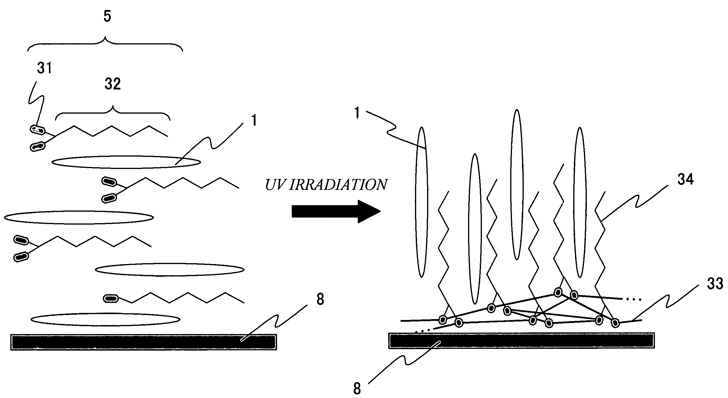
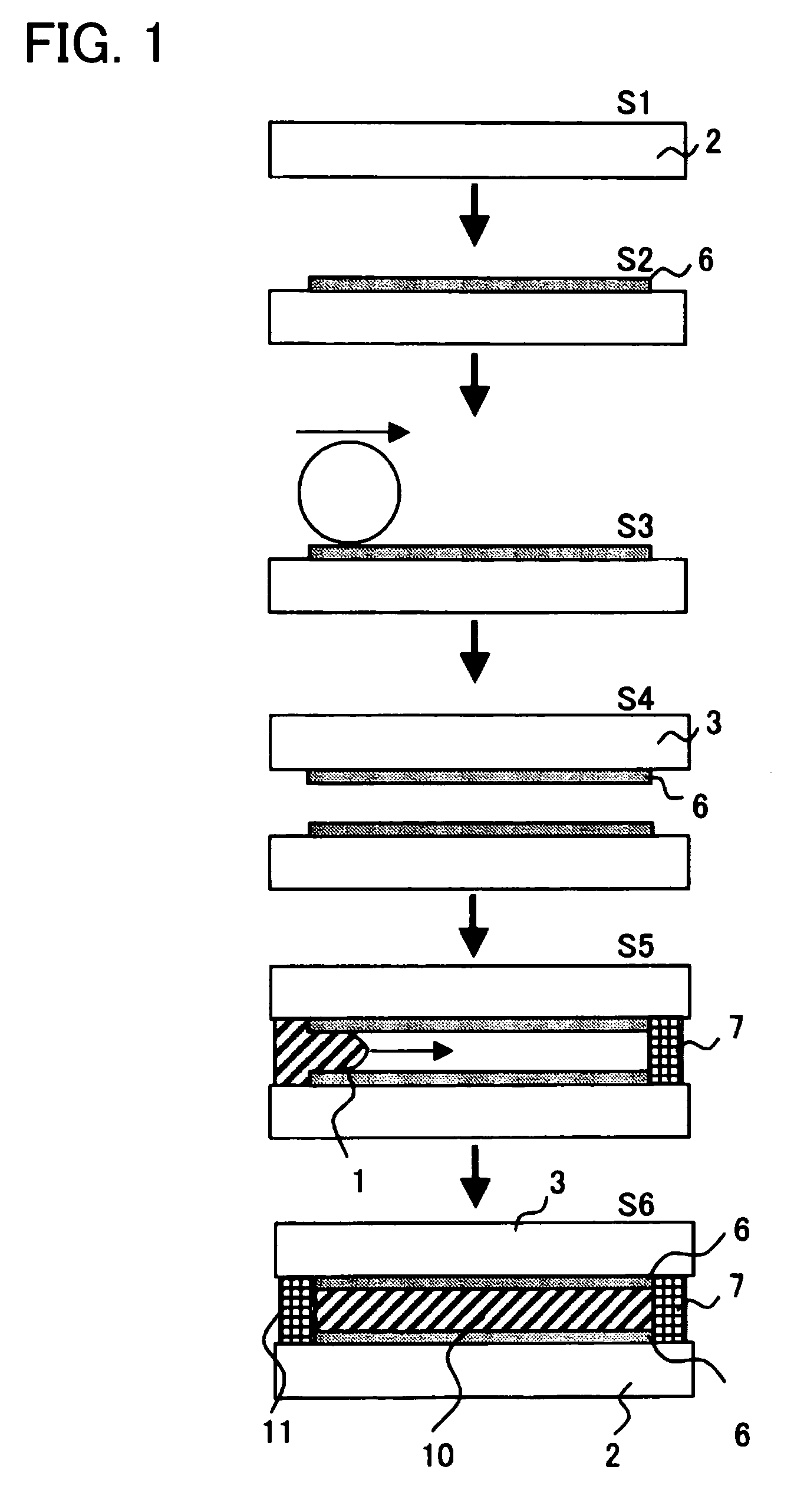
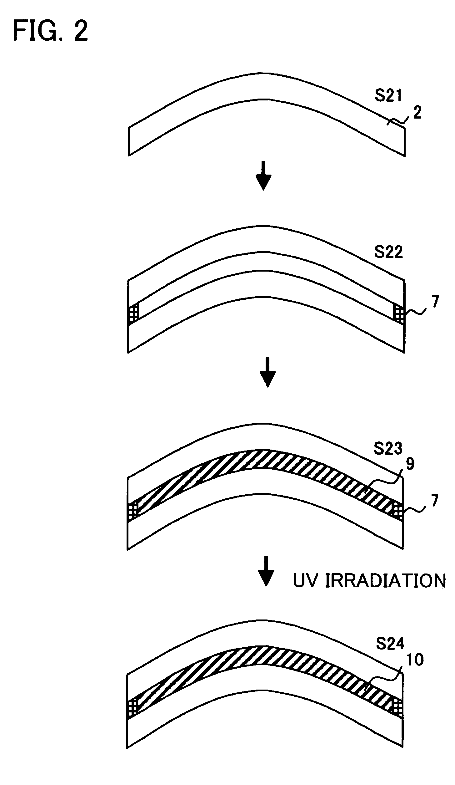
[0096]A 0.4 mm-thick polycarbonate substrate with an ITO (indium-tin oxide) transparent electrode that had been processed to have a curved surface with a curvature radius of 200 mm, and a 0.7 mm-thick glass substrate having the same curvature radius were bonded together using a thermosetting sealant, without forming an alignment control film, to form a blank cell.

[0097]A liquid crystal (liquid crystal D) made by Merck & Co., Inc. having a negative dielectric constant anisotropy as shown in TABLE 1 in an amount of 98 parts by weight was mixed with 2 parts by weight of an acrylate resin composition according to the present invention to form a liquid crystal mixture. For the resin composition according to the present invention, used was a mixture made by adding 2.5% by weight of a polymerization initiator Irgacure 651 made by Ciba-Geigy Specialty Chemicals Co. to the whole amount of a mixture obtained by mixing lauryl acrylate as a monofunctional monomer and HDDA (1,6-hexanediol diacry...

example 2

[0101]The same experiment as for EXAMPLE 1 was conducted to form a liquid crystal cell except that instead of liquid crystal D, various liquid crystals made by Merck & Co., Inc. as shown in TABLE 1 were used. When observed, this liquid crystal cell showed good, uniform, vertical alignment when no voltage was applied.

[0102]It is to be noted that TABLE 1 also shows data for EXAMPLE 1 with liquid crystal D. In TABLE 1, “negative, fluorinated” means that the corresponding liquid crystal is a fluorinated liquid crystal and has a negative dielectric constant anisotropy. TN-I indicates a transition point between a nematic phase and an isotropic phase, TS-N, a transition point between a smectic phase and a nematic phase, Δn, a refractive index anisotropy, Δε, a dielectric constant anisotropy, K11, an elastic coefficient (spray), K33, an elastic coefficient (bend), γ1, a rotational viscosity.

[0103]TABLE 1 shows that those negative, fluorinated liquid crystals had excellent effects.

[0104]

TABL...


PUM

PropertyMeasurementUnit
thicknessaaaaaaaaaa
thicknessaaaaaaaaaa
thickaaaaaaaaaa

Abstract

A liquid crystal panel is provided that has a liquid crystal layer sandwiched between a pair of substrates, wherein the liquid crystal layer comprises a liquid crystal and a cross-linked resin, the cross-linked resin comprises a cross-linked structural part adhered to a liquid crystal layer contacting surface and a terminal part rising from the liquid crystal layer contacting surface, and at least one of three conditions: the outer surface of at least one substrate is curved; a liquid crystal layer contacting surface is curved; and the thickness of one of the substrates is not more than ½ of the thickness of the other substrate, is satisfied. It is possible to obtain a liquid crystal panel having increased freedom in the appearance, device weight reduction, simplified structure, etc. by improving the outer and / or inner surfaces of the device.

Description

BACKGROUND OF THE INVENTION[0001]1. Field of the Invention[0002]The present invention relates to a liquid crystal panel with improved outer and / or inner surfaces.[0003]2. Description of the Related Art[0004]Conventional liquid crystal panels are flat panel displays manufactured by bonding together a pair of flat substrates represented by glass, or liquid crystal panels for which substrates such as plastic substrates are used.[0005]FIG. 1 is a model view illustrating the manufacturing flow for a conventional liquid crystal panel. Going down from the top of FIG. 1 to the bottom, first, a substrate 2 that has not an alignment control film coated thereon is prepared according to step S1, an alignment control film 6 composed of a polyimide or the like is formed on the substrate 2 according to step S2, substrate treating such as rubbing is optionally performed according to step S3, bonding with another substrate 3 is performed according to step S4, a liquid crystal is filled in the space ...

Claims


Application Information

Patent Timeline
Patent Type & Authority Patents(United States)
IPC IPC(8): C09K19/56G02F1/1334C09K19/54G02F1/1333G02F1/1337G02F1/1347G02F1/29
CPCC09K19/544G02F1/133788C09K2019/548G02F1/133305G02F1/133703Y10T428/10G02F1/29G02F2001/133368G02F2001/133742Y10T428/1005Y10T428/1036G02F1/1347C09K2323/00C09K2323/02C09K2323/03G02F1/133368G02F1/133742
Inventor TSUDA, HIDEAKITANUMA, SEIJIKOIKE, YOSHIO
Owner MERCK PATENT GMBH
Why Eureka
Try Eureka