Technique for forming a transistor having raised drain and source regions with a tri-layer hard mask for gate patterning

a technology of gate patterning and raised drain and source regions, which is applied in the direction of basic electric elements, electrical apparatus, semiconductor devices, etc., can solve the problems of reduced pn junction size, low pattern fidelity, and inability to completely activate the dopant implanted in these regions at very high concentrations, so as to achieve reliable coverage of the top surface of the gate electrode structure and high pattern fidelity

Active Publication Date: 2007-10-09
TAIWAN SEMICON MFG CO LTD
View PDF6 Cites 2 Cited by
  • Summary
  • Abstract
  • Description
  • Claims
  • Application Information

AI Technical Summary

Benefits of technology

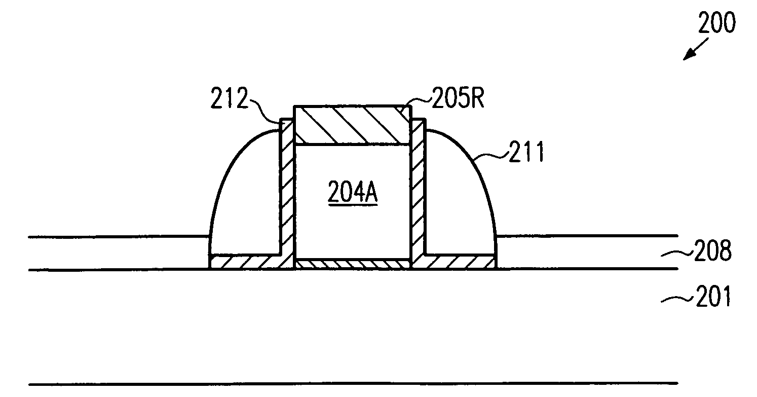
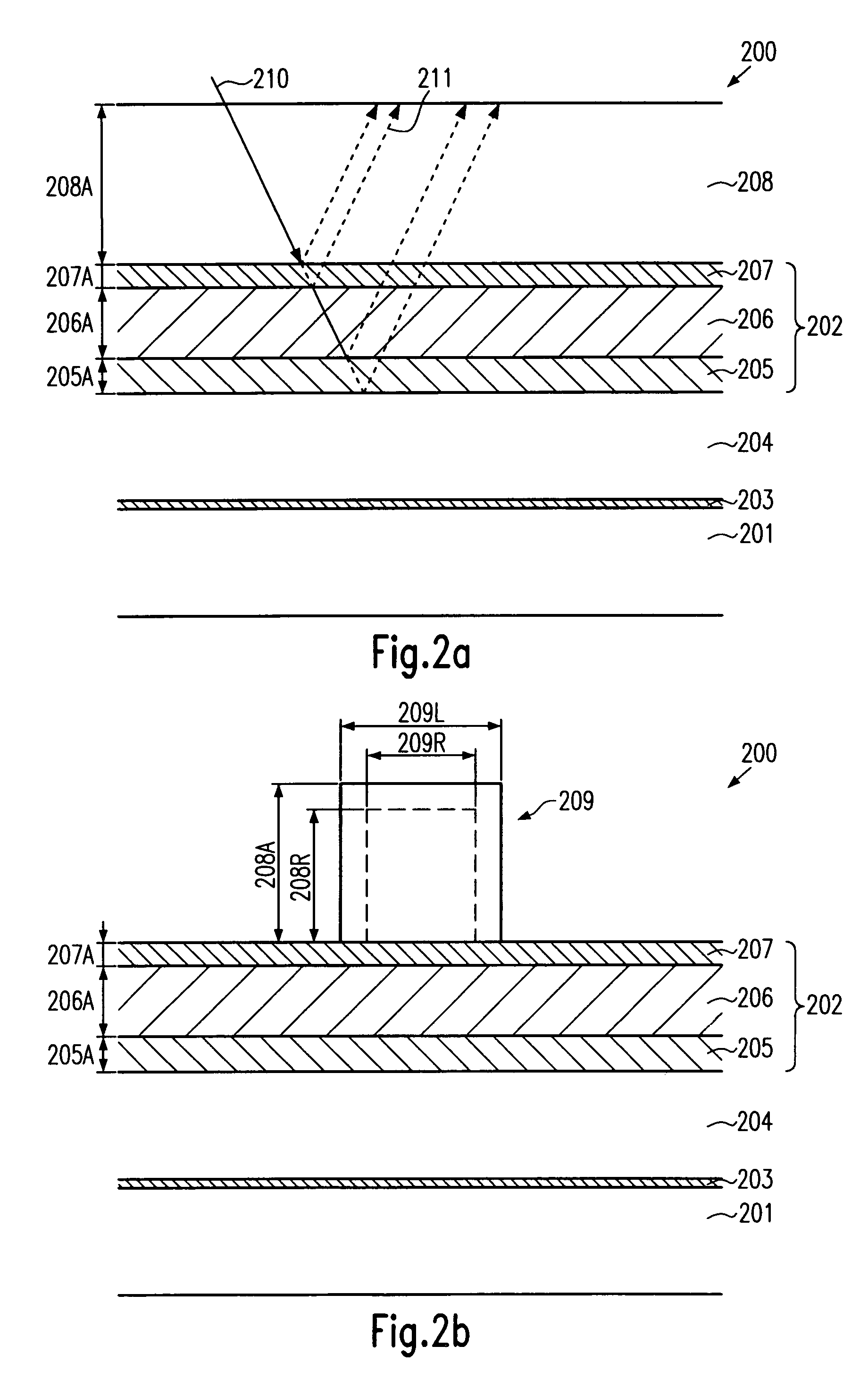
[0022]Generally, the present invention is directed to a technique that enables the formation of advanced transistor devices requiring raised drain and source regions formed by a selective epitaxial growth technique, wherein, at the same time, the patterning process for forming the gate electrode structure may be performed with high pattern fidelity even for highly scaled devices, while, after the patterning process, a reliable coverage of the top surface of the gate electrode structure is obtained. For this purpose, a hard mask layer is provided for patterning the gate electrode structure, wherein the hard mask layer may comprise a specified layer designed to substantially remain intact after the patterning process.

Problems solved by technology

The shrinkage of the transistor dimensions, however, entails a plurality of issues associated therewith which have to be addressed so as to not unduly offset the advantages obtained by steadily decreasing the channel length of MOS transistors.
One problem in this respect is the requirement of extremely shallow PN junctions.
The depth of the source and drain regions substantially determines the sheet resistance thereof, which may not be arbitrarily reduced by correspondingly increasing the dopant concentration in the source and drain regions, since an extremely high dopant concentration may give rise to increased leakage currents.
Furthermore, the dopants implanted into these regions at very high concentrations may not be completely activated by conventional rapid thermal anneal processes without negatively affecting the overall dopant profile within the source and drain regions.
That is, for a desired channel length, defined by the PN junctions, an increased dopant concentration requires higher temperatures and / or a prolonged duration of the corresponding anneal cycles, thereby, however, influencing the dopant profile forming the PN junctions by the inevitable thermal diffusion of the dopants, which finally may lead to a non-acceptable variation of the finally achieved channel length.
However, since the penetration depth of the metal silicide is restricted by the depth of the PN junctions, the improvement in conductivity in these regions is therefore coupled to the depth of the corresponding PN junctions.
Moreover, in many CMOS technologies, a corresponding metal silicide is simultaneously formed on the gate electrode, wherein a shallow junction depth therefore also creates a very shallow metal silicide in the gate electrode, thereby providing only limited improvement in gaining superior gate electrode conductivity.
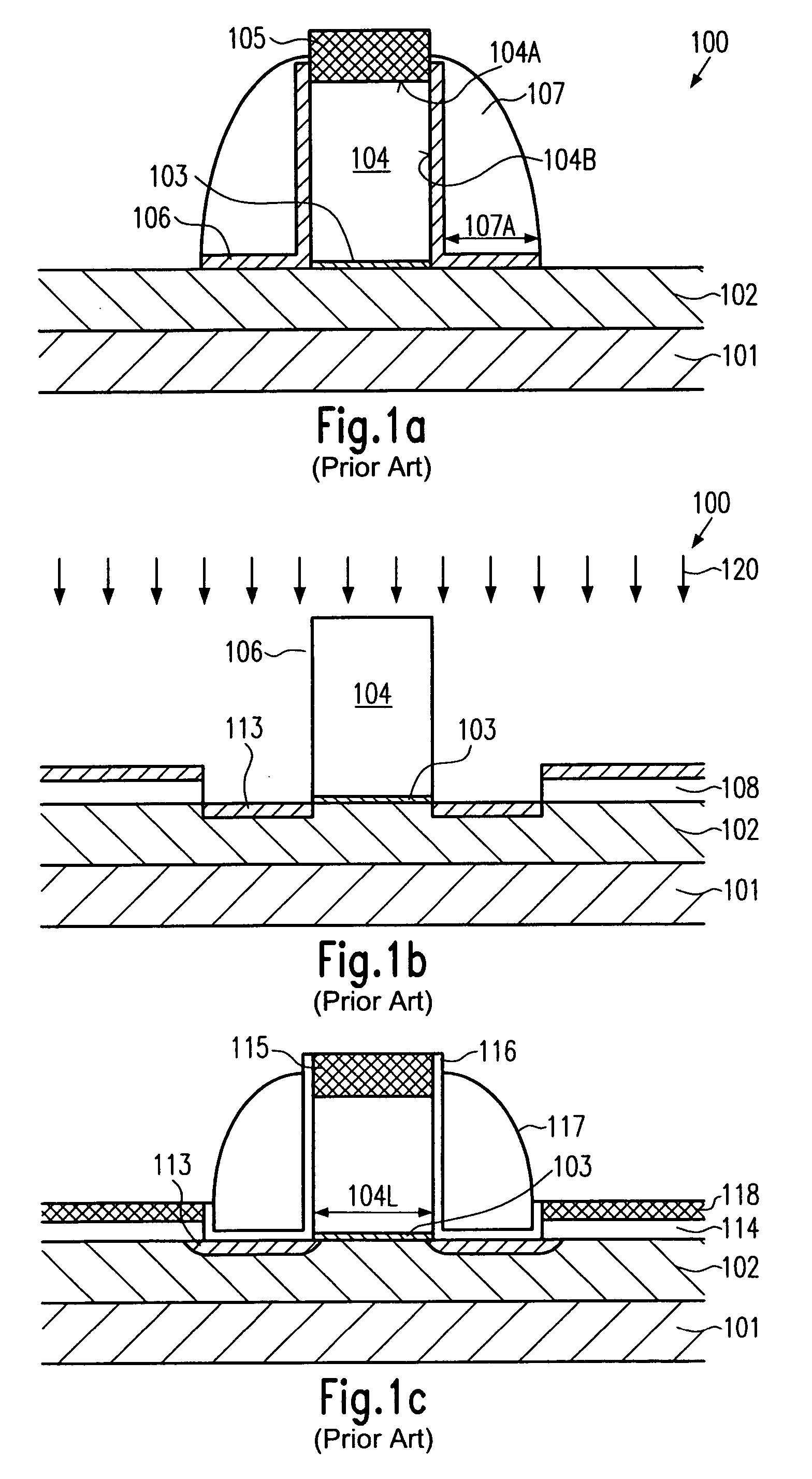
Consequently, the coverage of the top surface 104a with an ARC layer meeting the strict requirements of the preceding lithography, resist trim and gate etch processes designed for highly scaled devices may not be reliably guaranteed.

Method used


Image

  • Technique for forming a transistor having raised drain and source regions with a tri-layer hard mask for gate patterning
  • Technique for forming a transistor having raised drain and source regions with a tri-layer hard mask for gate patterning
  • Technique for forming a transistor having raised drain and source regions with a tri-layer hard mask for gate patterning

Examples


Embodiment Construction

[0029]Illustrative embodiments of the invention are described below. In the interest of clarity, not all features of an actual implementation are described in this specification. It will of course be appreciated that in the development of any such actual embodiment, numerous implementation-specific decisions must be made to achieve the developers' specific goals, such as compliance with system-related and business-related constraints, which will vary from one implementation to another. Moreover, it will be appreciated that such a development effort might be complex and time-consuming, but would nevertheless be a routine undertaking for those of ordinary skill in the art having the benefit of this disclosure.

[0030]The present invention will now be described with reference to the attached figures. Various structures, systems and devices are schematically depicted in the drawings for purposes of explanation only and so as to not obscure the present invention with details that are well ...


PUM


Abstract

By providing a hard mask layer stack including at least three different layers for patterning a gate electrode structure, constraints demanded by sophisticated lithography, as well as cap layer integrity, in a subsequent selective epitaxial growth process may be accomplished, thereby providing the potential for further device scaling of transistor devices requiring raised drain and source regions.

Description

BACKGROUND OF THE INVENTION[0001]1. Field of the Invention[0002]The present invention generally relates to the fabrication of integrated circuits, and, more particularly, to the formation of field effect transistors having epitaxially grown raised drain and source regions so as to provide extremely shallow PN junctions.[0003]2. Description of the Related Art[0004]The fabrication of integrated circuits requires the formation of a large number of circuit elements on a given chip area according to a specified circuit layout. Generally, a plurality of process technologies are currently practiced, wherein, for logic circuitry, such as microprocessors, storage chips and the like, CMOS technology is currently the most promising approach, due to the superior characteristics in view of operating speed and / or power consumption and / or cost efficiency. During the fabrication of complex integrated circuits using CMOS technology, millions of complementary transistors, i.e., N-channel transistors ...

Claims


Application Information

Patent Timeline
Patent Type & Authority Patents(United States)
IPC IPC(8): H01L21/336
CPCH01L21/32139H01L29/7834H01L29/66628H01L21/823814H01L29/6656
Inventor ROMERO, KARLAKAMMLER, THORSTENLUNING, SCOTTVAN MEER, HANS
Owner TAIWAN SEMICON MFG CO LTD
Why Eureka
Try Eureka